Optoelectronic devices having arrays of quantum-dot compound semiconductor superlattices therein

a quantum-dot compound and semiconductor superlattice technology, applied in the direction of superimposed coating process, nanoinformatics, coatings, etc., can solve the problems of moore's law predicted performance improvement, inhibiting further scaling of conventional devices, and affecting the lowering of drain-induced barrier of thin-body soi transistors, so as to reduce the number of photolithographically defined processing steps

Inactive Publication Date: 2005-07-05
NORTH CAROLINA STATE UNIV
View PDF15 Cites 143 Cited by
  • Summary
  • Abstract
  • Description
  • Claims
  • Application Information

AI Technical Summary

Benefits of technology

[0011]Embodiments of the present invention include nano-scale electronic devices and methods of forming nano-scale electronic devices using techniques that advantageously have a reduced number of photolithographically defined processin

Problems solved by technology

As semiconductor devices scale down to nano-scale dimensions (i.e., ≦100 nm features), the performance improvements predicted by Moore's Law typically diminish.
Some fundamental physical properties, such as direct quantum tunneling through gate dielectrics, poly depletion in gate electrodes and source-drain leakage due to short channel effects, may become limiting factors in performance and may inhibit further scaling of conventional devices.
However, the thin-body SOI tr

Method used


Image

  • Optoelectronic devices having arrays of quantum-dot compound semiconductor superlattices therein
  • Optoelectronic devices having arrays of quantum-dot compound semiconductor superlattices therein
  • Optoelectronic devices having arrays of quantum-dot compound semiconductor superlattices therein

Examples


Embodiment Construction

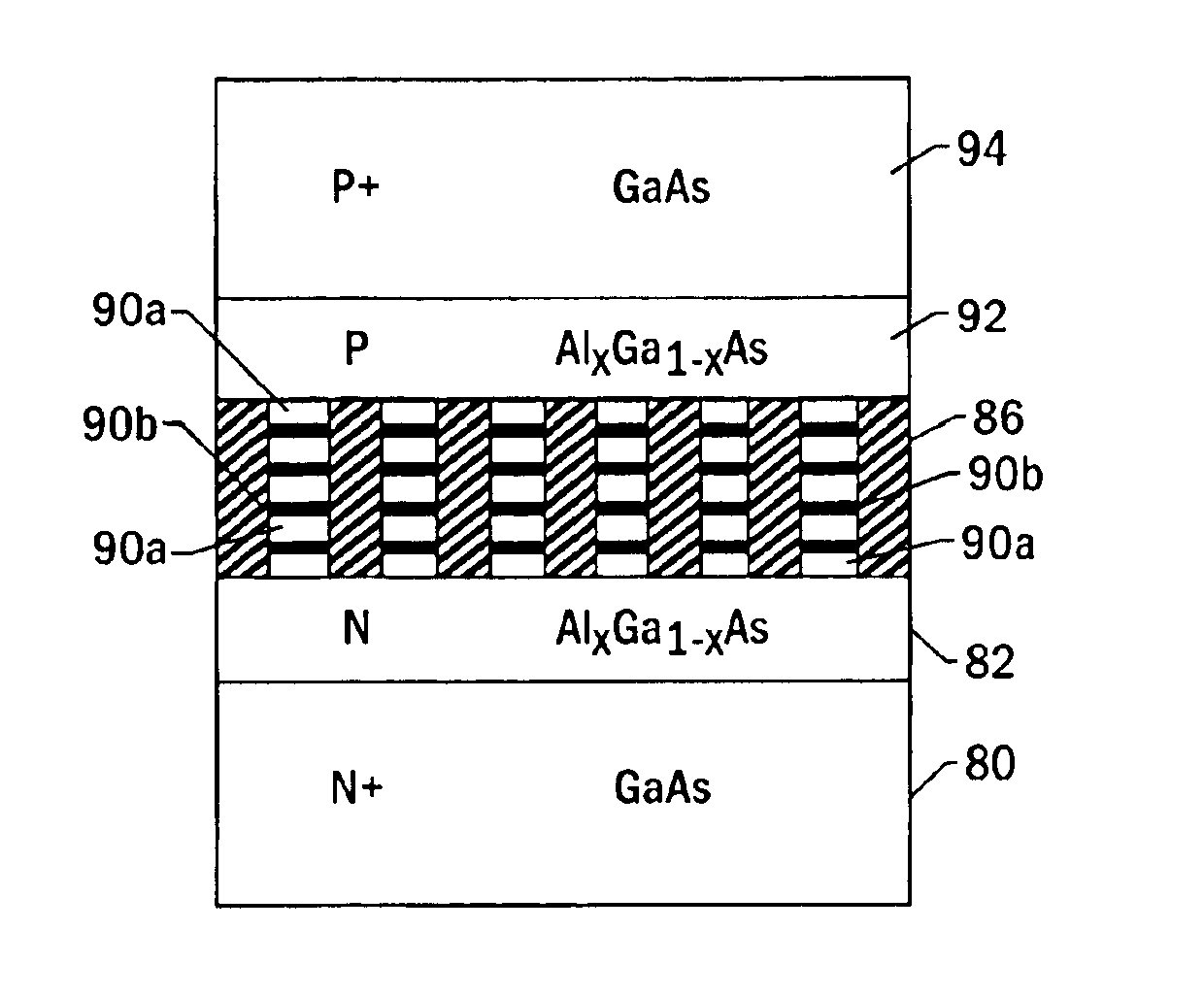
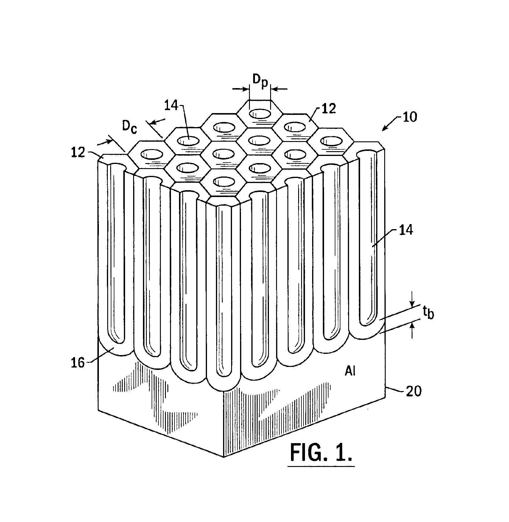
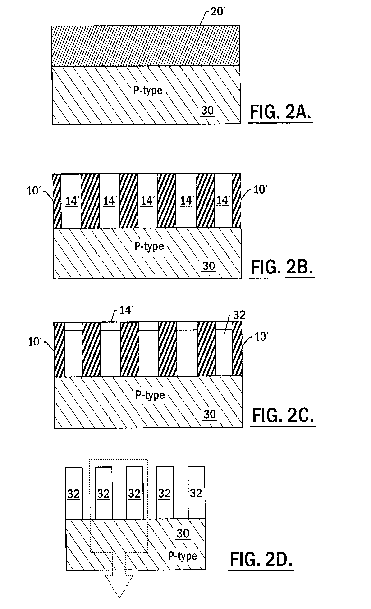
[0024]The present invention will now be described more fully hereinafter with reference to the accompanying drawings, in which preferred embodiments of the invention are shown. This invention may, however, be embodied in different forms and should not be construed as limited to the embodiments set forth herein. Rather, these embodiments are provided so that this disclosure will be thorough and complete, and will fully convey the scope of the invention to those skilled in the art. In the drawings, the thickness of layers and regions are exaggerated for clarity. It will also be understood that when a layer is referred to as being “on” another layer or substrate, it can be directly on the other layer or substrate, or intervening layers may also be present. Moreover, the terms “first conductivity type” and “second conductivity type” refer to opposite conductivity types such as N or P-type, however, each embodiment described and illustrated herein includes its complementary embodiment as...


PUM

PropertyMeasurementUnit
Diameteraaaaaaaaaa
Diameteraaaaaaaaaa
aaaaaaaaaa

Abstract

Methods of forming a nano-scale electronic and optoelectronic devices include forming a substrate having a semiconductor layer therein and a substrate insulating layer on the semiconductor layer. An etching template having a first array of non-photolithographically defined nano-channels extending therethrough, is formed on the substrate insulating layer. This etching template may comprise an anodized metal oxide, such as an anodized aluminum oxide (AAO) thin film. The substrate insulating layer is then selectively etched to define a second array of nano-channels therein. This selective etching step preferably uses the etching template as an etching mask to transfer the first array of nano-channels to the underlying substrate insulating layer, which may be thinner than the etching template. An array of semiconductor nano-pillars is then formed in the second array of nano-channels. The semiconductor nano-pillars in the array may have an average diameter in a range between about 8 nm and about 50 nm. The semiconductor nano-pillars are also preferably homoepitaxial or heteroepitaxial with the semiconductor layer.

Description

REFERENCE TO PRIORITY APPLICATIONS[0001]This application is a divisional of U.S. application Ser. No. 10 / 178,941, filed Jun. 24, 2002 now U.S. Pat. No. 6,769,929, which derives priority from Provisional Application Ser. Nos. 60 / 300,804, filed Jun. 25, 2001 and 60 / 301,018, filed Jun. 26, 2001, the disclosures of which are hereby incorporated herein by reference.GOVERNMENT RIGHTS[0002]This invention was made with Government support under Contract No. N66001-01-1-8977, awarded by SPAWAR / DARPA. The Government may have certain rights in this invention.FIELD OF THE INVENTION[0003]The present invention relates to methods of forming integrated circuit devices and device formed thereby and, more particularly, to methods of forming integrated circuit devices having nano-scale features therein and integrated circuit devices formed thereby.BACKGROUND OF THE INVENTION[0004]As semiconductor devices scale down to nano-scale dimensions (i.e., ≦100 nm features), the performance improvements predicte...

Claims


Application Information

Patent Timeline
IPC IPC(8): H01L29/06H01L21/20H01L21/02H01L29/12H01L29/02
CPCB82Y10/00H01L29/0665H01L29/0673H01L29/0676H01L29/068H01L29/125H01L29/127H01L21/02381H01L21/02395H01L21/02463H01L21/02488H01L21/02546H01L21/0262H01L21/02642Y10S977/762
Inventor ZHANG, ZHIBOMISRA, VEENABEDAIR, SALAH M. A.OZTURK, MEHMET
Owner NORTH CAROLINA STATE UNIV
Why Eureka
Try Eureka