Method of selective epitaxy

a selective epitaxy and film technology, applied in the direction of semiconductor devices, basic electric elements, electrical equipment, etc., can solve the problems of poor electrical properties, high defect concentration, and difficult epitaxial growth

Inactive Publication Date: 2018-02-15
APPLIED MATERIALS INC
View PDF12 Cites 3 Cited by
  • Summary
  • Abstract
  • Description
  • Claims
  • Application Information

AI Technical Summary

Problems solved by technology

This phenomenon makes it very challenging for epitaxial growth in narrow trenches with silicon oxide sidewall, while having the same growth selective to silicon nitride areas on the sidewall.
The surface morphology of the epitaxial material is suffered due to the formation of the facets, resulting in a higher concentration of the defects and poor electrical properties.

Method used


Image

  • Method of selective epitaxy
  • Method of selective epitaxy
  • Method of selective epitaxy

Examples


Embodiment Construction

[0013]Embodiments of the present disclosure provide methods for manufacturing semiconductor devices such as transistors used for amplifying or switching electronic signals. For example, the disclosed methods may be utilized in the manufacture of CMOS (Complementary Metal-Oxide-Semiconductor) transistors. While embodiments described in this disclosure use a general term “integrated circuit” as an example, it should be understood that these embodiments are equally applicable to any integrated circuit technologies such as bipolar, N-type or P-type metal oxide semiconductor (NMOS or PMOS), or CMOS etc. Particularly, embodiments of the present disclosure can benefit processes of fabricating NMOS / PMOS inverters or gates, CMOS inverters or gates, any integral circuit devices incorporating a gate structure, or any integral circuit devices having transistors (2D or 3D) or multiple gate structures.

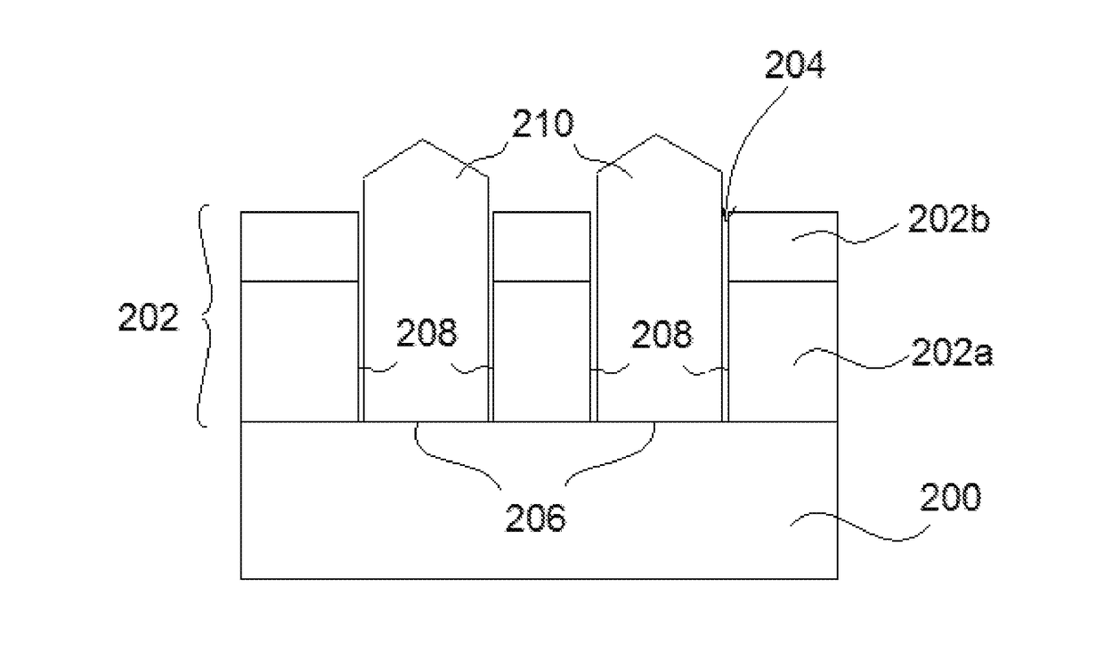
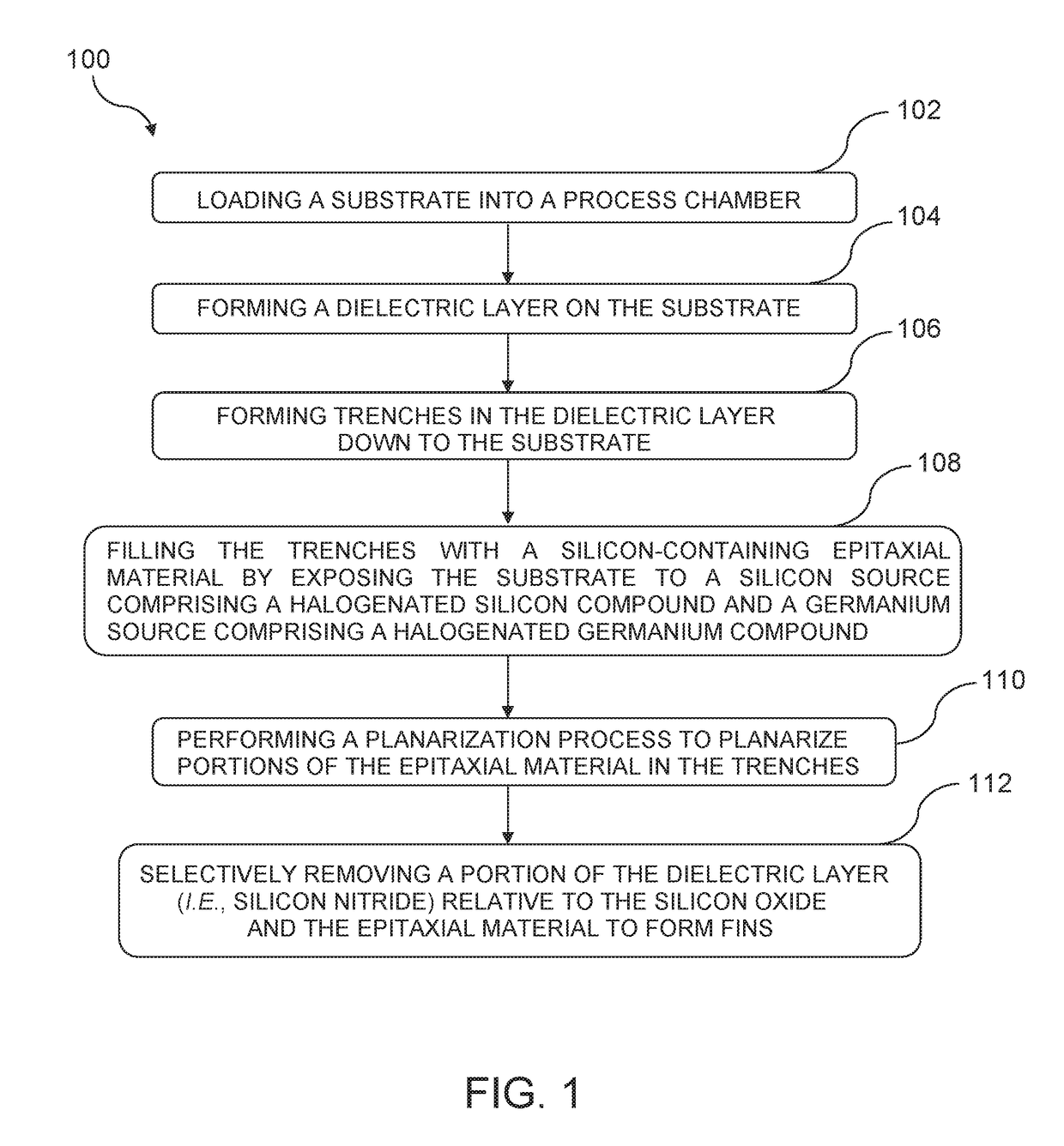
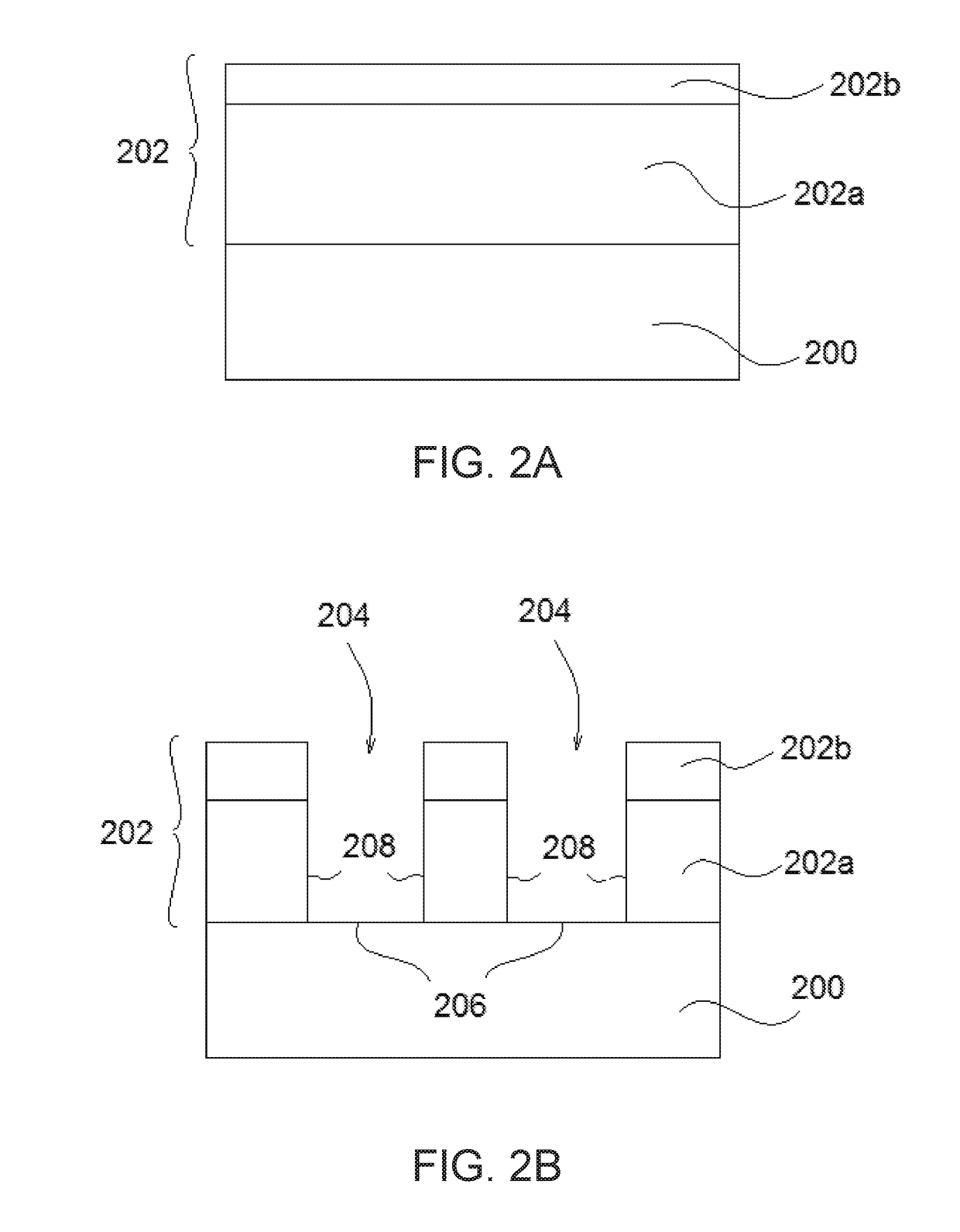
[0014]FIG. 1 depicts a flow chart illustrating an exemplary method 100 for manufacturing an inte...


PUM

PropertyMeasurementUnit
temperatureaaaaaaaaaa
widthaaaaaaaaaa

Abstract

Embodiments of the present disclosure generally relate to methods for trench filling of high quality epitaxial silicon-containing material without losing selectivity of growth to dielectrics such as silicon oxides and silicon nitrides. The methods include epitaxially growing a silicon-containing material within a trench formed in a dielectric layer by exposing the trench to a gas mixture comprising a halogenated silicon compound and a halogenated germanium compound. In one embodiment, the halogenated silicon compound includes chlorinated silane and halogenated germanium compound includes chlorinated germane.

Description

CROSS-REFERENCE TO RELATED APPLICATIONS[0001]This application is a divisional of U.S. patent application Ser. No. 15 / 156,870, filed May 17, 2016, which claims priority to U.S. provisional patent application Ser. No. 62 / 192,801, filed Jul. 15, 2015, both applications are hereby incorporated by reference.BACKGROUNDField[0002]Embodiments of the disclosure generally relate to the field of semiconductor manufacturing processes and devices, more particularly, to methods of depositing silicon-containing films for forming semiconductor devices.Description of the Related Art[0003]Semiconductor industry is in the era of transitioning from 2D transistors, which are often planar, to 3D transistors using a three-dimensional gate structure. In 3D gate structures, the channel, source and drain are raised out of the substrate and the gate is then wrapped around the channel on three sides. The goal is to constrain the current to only the raised channel, and abolish any path through which electrons m...

Claims


Application Information

Patent Timeline
Patent Type & Authority Applications(United States)
IPC IPC(8): H01L21/02H01L21/311
CPCH01L21/02381H01L21/02642H01L21/02639H01L21/0262H01L21/02579H01L21/02576H01L21/0217H01L21/02164H01L21/02532H01L21/02433H01L21/31105H01L29/66795H01L21/02293H01L29/4236H01L29/7831H01L29/785
Inventor HUANG, YI-CHIAUCHUNG, HUADUBE, ABHISHEK
Owner APPLIED MATERIALS INC
Why Eureka
Try Eureka