Method for forming a low thermal budget spacer

a low-temperature budget and spacer technology, applied in the direction of basic electric elements, electrical apparatus, semiconductor devices, etc., can solve the problems of short channel and punch-through effects, difficult to control the adverse electrical effects, and increase the power consumption of transistors

Inactive Publication Date: 2006-05-23
APPLIED MATERIALS INC
View PDF16 Cites 235 Cited by
  • Summary
  • Abstract
  • Description
  • Claims
  • Application Information

AI Technical Summary

Problems solved by technology

When dopants (e.g., boron) migrate upward it sets up concentration gradients in the underlying source or drain region, which can cause parasitic junctions that increase power consumption by the transistor.
Extensive thermal diffusion can also cause the dopant region to close or overlap each other causing short channel and punch-through effects.
However, with conventional methods of forming the SiO2 / Si3N4 layers (i.e., LPCVD) it is difficult to control the adverse electrical effects that arise from impurity diffusion.

Method used


Image

  • Method for forming a low thermal budget spacer
  • Method for forming a low thermal budget spacer
  • Method for forming a low thermal budget spacer

Examples


Embodiment Construction

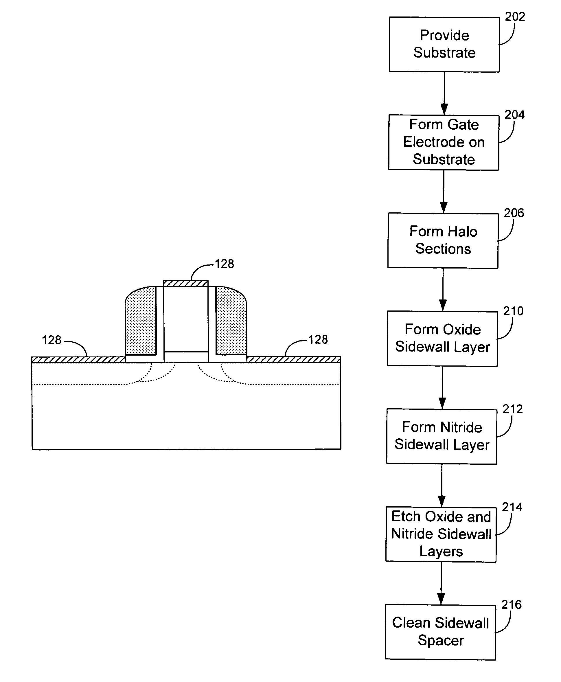
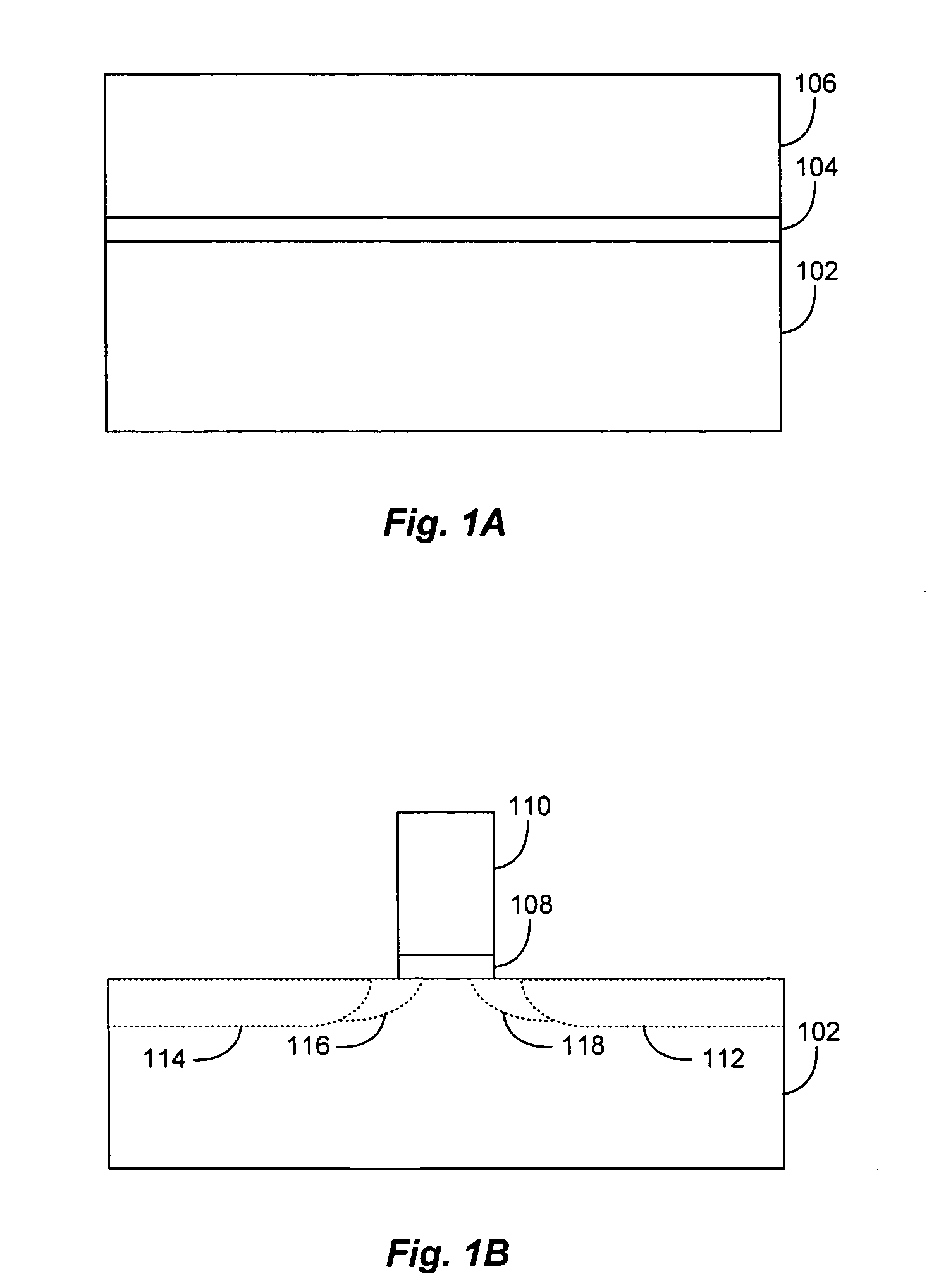
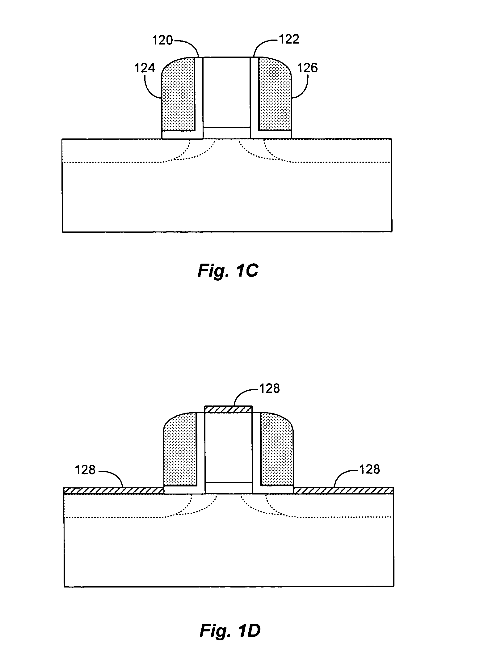
[0016]As noted above, the shrinking sizes of transistors require precise positioning of the transistor elements that define the channel region. These elements include the source and drain regions formed in the substrate. They also include counter-doped regions (e.g., halo sections) that may be formed at the ends of the source and drain regions and may define the length of the channel region.

[0017]As the channel regions of transistors get shorter the migration of dopants in the source and drain regions and halo sections becomes more problematic. The probability increases that dopants will migrate from the source region to the drain region (or from opposite halo sections), weakening the ability of the transistor control current flow through the channel region. In some circumstances, dopant migration may be severe enough to cause a disabling short circuit in the transistor (e.g., a short between the gate electrode and source or drain region).

[0018]One aspect of controlling dopant migra...


PUM


Abstract

A method of forming a sidewall spacer on a gate electrode of a metal oxide semiconductor device that includes striking a first plasma to form an oxide layer on a side of the gate electrode, where the first plasma is generated from a oxide gas that includes O3 and bis-(tertiarybutylamine)silane, and striking a second plasma to form a carbon-doped nitride layer on the oxide layer, where the second plasma may be generated from a nitride gas that includes NH3 and the bis-(tertiarybutylamine)silane. The first and second plasmas may be formed using plasma CVD and the bis-(tertiarybutylamine)silane flows uninterrupted between the striking of the first plasma and the striking of the second plasma.

Description

BACKGROUND OF THE INVENTION[0001]Many modern semiconductor devices are composed of MOS (Metal-Oxide-Semiconductor) transistors and capacitors, in which the MOS transistors generally include a source, drain, and gate. The gate is sometimes called a gate stack because it may include a plurality of components components, such as a gate electrode and an underlying gate dielectric. Sidewall spacers (also called spacers, or spacer layers) may be adjacent to the gate structure and usually include an oxide layer and a nitride layer component.[0002]Spacers serve a number of functions in the formation of semiconductor devices. One function of spacers is to assist in the alignment of silicide layers above the source-drain regions and the gate electrode. Silicide layers are highly conductive compared to the underlying source-drain regions and gate electrode, and facilitate the transfer of electric signals to and from the transistor. The silicide layers are formed by depositing a metal layer (e....

Claims


Application Information

Patent Timeline
Patent Type & Authority Patents(United States)
IPC IPC(8): H01L21/336H01L21/28H01L21/314H01L21/316H01L21/318
CPCH01L21/02126H01L21/02164H01L21/0217H01L21/3185H01L21/02274H01L21/3145H01L21/31612H01L21/022
Inventor ARGHAVANI, REZAMACWILLIAMS, KENM'SAAD, HICHEM
Owner APPLIED MATERIALS INC
Why Eureka
Try Eureka