Film formation method and apparatus for semiconductor process

a film formation and semiconductor technology, applied in the field of film formation methods and apparatus for semiconductor processes, can solve the problems of low etching resistance, low dielectric constant, and increased parasitic capacitance, and achieve the effect of high etching resistance and low dielectric constan

Active Publication Date: 2006-02-16
TOKYO ELECTRON LTD
View PDF3 Cites 275 Cited by
  • Summary
  • Abstract
  • Description
  • Claims
  • Application Information

AI Technical Summary

Benefits of technology

[0010] An object of the present invention is to provide a film formation method and apparatus for a semiconductor process, which can form a film of silicon nitride or silicon oxynitride doped with an impurity and having a low dielectric constant and a high etching resistance.

Problems solved by technology

In this respect, silicon nitride films have a relatively high dielectric constant, which increases parasitic capacitance and thus is problematic.
Further, where a silicon nitride film is used for a sensor of the charge storage type, there is a problem in that parasitic capacitance increases a background level.
However, silicon nitride films doped with boron, which are formed by CVD, have a relatively low strength and a low etching resistance.
As a consequence, for example, when dry etching is performed in a subsequent step, silicon nitride films doped with boron tend to be excessively etched.

Method used


Image

  • Film formation method and apparatus for semiconductor process
  • Film formation method and apparatus for semiconductor process
  • Film formation method and apparatus for semiconductor process

Examples


first embodiment

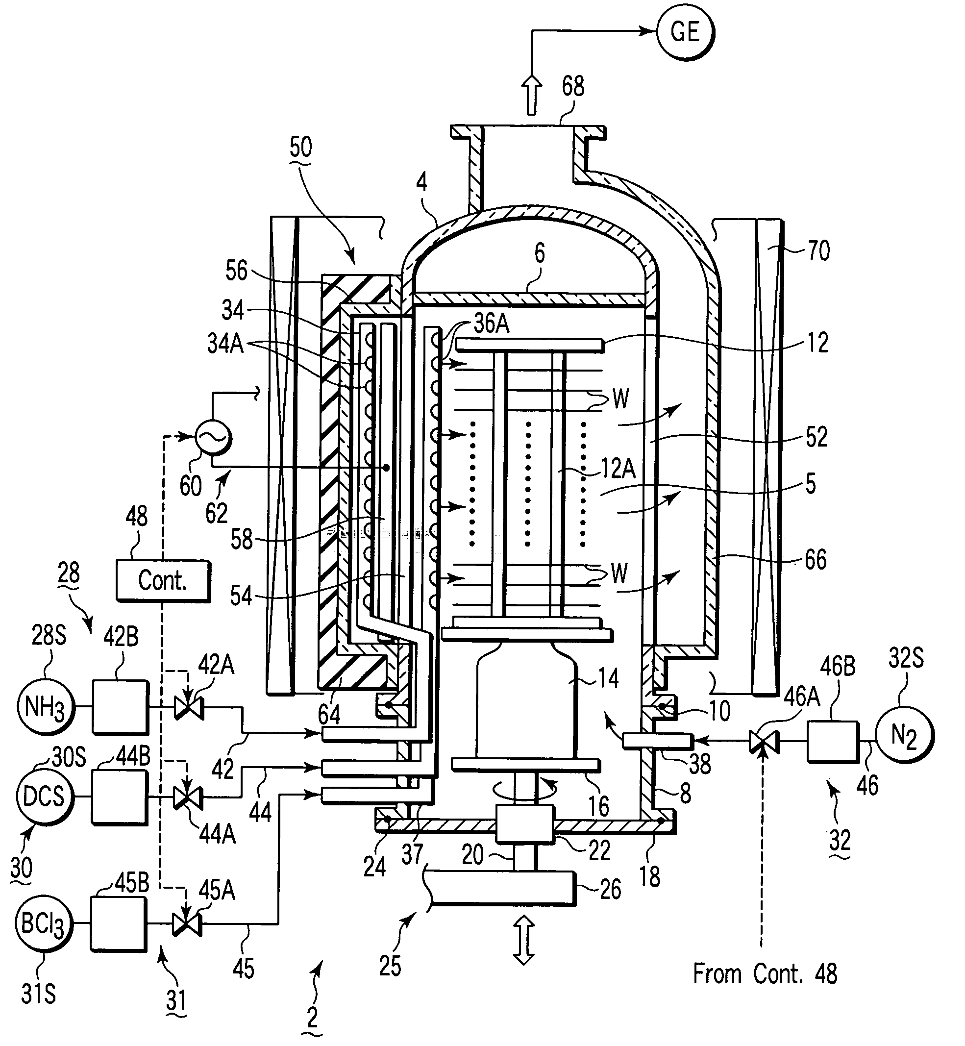
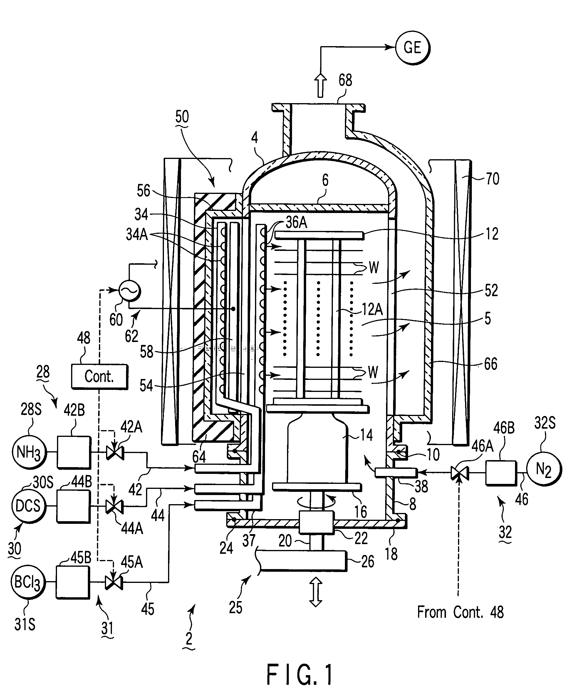
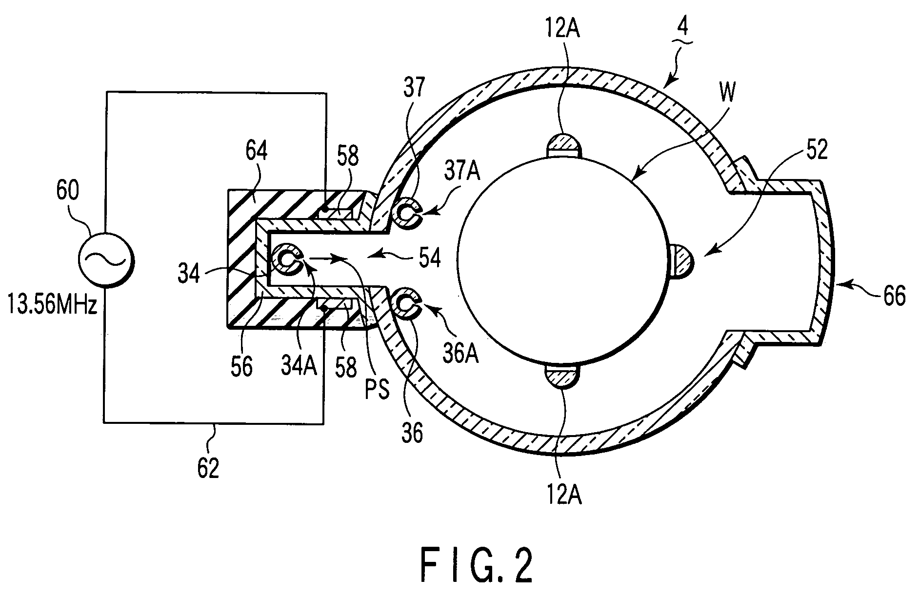
[0076]FIG. 3 is a timing chart of the gas supply and RF (radio frequency) application of a film formation method according to a first embodiment of the present invention. As shown in FIG. 3, the film formation method according to this embodiment is arranged to alternately repeat first to fourth steps T1 to T4. A cycle comprising the first to fourth steps T1 to T4 is repeated a number of times, and thin films of silicon nitride doped with boron formed by respective cycles are laminated, thereby arriving at a silicon nitride film having a target thickness.

[0077] Specifically, the first step T1 is arranged to perform supply of the source gas (denoted as DCS in FIG. 3) and the supplementary gas (denoted as BCl3 in FIG. 3) to the process field 5, while stopping supply of the assist gas (denoted as NH3 in FIG. 3) to the process field 5. The second step T2 is arranged to stop supply of the source gas, assist gas, and supplementary gas to the process field 5. The third step T3 is arranged ...

second embodiment

[0102]FIG. 8 is a timing chart of the gas supply and RF (radio frequency) application of a film formation method according to a second embodiment of the present invention. As shown in FIG. 8, the film formation method according to this embodiment is also arranged to alternately repeat first to fourth steps T11 to T14. A cycle comprising the first to fourth steps T11 to T14 is repeated a number of times, and thin films of silicon nitride doped with boron formed by respective cycles are laminated, thereby arriving at a silicon nitride film having a target thickness.

[0103] Specifically, the first step T11 is arranged to perform supply of the source gas (denoted as DCS in FIG. 8), the assist gas (denoted as NH3 in FIG. 8), and the supplementary gas (denoted as BCl3 in FIG. 8) to the process field 5. The second step T12 is arranged to stop supply of the source gas, assist gas, and supplementary gas to the process field 5. The third step T13 is arranged to perform supply of the assist ga...


PUM

PropertyMeasurementUnit
stressaaaaaaaaaa
diameteraaaaaaaaaa
frequencyaaaaaaaaaa

Abstract

An impurity-doped silicon nitride or oxynitride film is formed on a target substrate by CVD, in a process field to be selectively supplied with a first process gas containing a silane family gas, a second process gas containing a nitriding or oxynitriding gas, and a third process gas containing a doping gas. This method alternately includes first to fourth steps. The first step performs supply of the first and third process gases to the field. The second step stops supply of the first to third process gases to the field. The third step performs supply of the second process gas to the field while stopping supply of the first and third process gases to the field, and includes an excitation period of exciting the second process gas by an exciting mechanism. The fourth step stops supply of the first to third process gases to the field.

Description

CROSS-REFERENCE TO RELATED APPLICATIONS [0001] This application is based upon and claims the benefit of priority from the prior Japanese Patent Applications No. 2004-220555, filed Jul. 28, 2004; No. 2005-048060, filed Feb. 23, 2005; and No. 2005-177344, filed Jun. 17, 2005, the entire contents of all of which are incorporated herein by reference. BACKGROUND OF THE INVENTION [0002] 1. Field of the Invention [0003] The present invention relates to a film formation method and apparatus for a semiconductor process for forming a film of silicon nitride or silicon oxynitride doped with an impurity on a target substrate, such as a semiconductor wafer. The term “semiconductor process” used herein includes various kinds of processes which are performed to manufacture a semiconductor device or a structure having wiring layers, electrodes, and the like to be connected to a semiconductor device, on a target substrate, such as a semiconductor wafer or a glass substrate used for an LCD (Liquid Cr...

Claims


Application Information

Patent Timeline
Patent Type & Authority Applications(United States)
IPC IPC(8): C23C16/00
CPCC23C16/30C23C16/345C23C16/45525C23C16/507C23C16/45546C23C16/45578C23C16/45531C23C16/45542C23C16/45553C23C16/45576H01L21/02126H01L21/02167H01L21/02208H01L21/02274H01L21/0228
Inventor HASEBE, KAZUHIDEOKADA, MITSUHIROCHOU, PAO-HWAKIM, CHAEHOOGAWA, JUN
Owner TOKYO ELECTRON LTD
Why Eureka
Try Eureka