Method of mass transferring electronic device

a technology of electronic devices and mass transfer, applied in the direction of solid-state devices, electric devices, basic electric elements, etc., can solve the problems of difficult to accurately align the micro light emitting diodes, over-long process time, and high cost, and achieve the effect of rapid and accurate mass transfer

Active Publication Date: 2018-02-22
GENESIS PHOTONICS
View PDF7 Cites 26 Cited by
  • Summary
  • Abstract
  • Description
  • Claims
  • Application Information

AI Technical Summary

Benefits of technology

[0005]The invention is directed to methods of mass transferring electronic devices, which are capable of rapidly and accurately transferring mass electronic devices.

Problems solved by technology

Also, it is difficult to accurately align the micro light emitting diodes since the device size is real small.
Therefore, if the micro light emitting diode needs to be aligned on a backplane of the display panel after being individually picked up, the cost is higher and the process time is overly long.
On the hand, if all the micro light emitting diodes are directly transferred onto the backplane of the display panel in large area, the micro light emitting diodes may not be electrically connected to the backplane successfully due to poor alignment, which then leads to generation of defect pixels.
Consequently, a manufacturing yield rate of the micro light emitting diode display panel will be reduced so that the development of the micro light emitting diode display panel is limited accordingly.

Method used


Image

  • Method of mass transferring electronic device
  • Method of mass transferring electronic device
  • Method of mass transferring electronic device

Examples


first embodiment

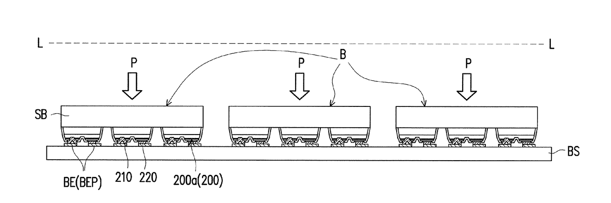
[0048]With reference to FIG. 6A and FIG. 6B, by applying an instantaneous force to the second surface S2 of the substrate 112 along the marks M with use of a splitting apparatus 130, the wafer 110 may be split into the blocks B on the temporary fixed layer 120. The splitting apparatus 130 is embodied as a chopper herein. The block B formed after splitting the wafer 110 may be regarded as one electronic device unit (e.g., one micro light emitting diode unit) including multiple electronic devices 200, such as the micro light emitting diode, for example. In the present embodiment, the number of the micro light emitting diodes 200a included by each of the blocks B falls within, for example, a range of 1 to 5×10⁶, but the invention is not limited thereto. At this point, description regarding the first method for cutting the wafer 110 according to the invention is substantially complete.

[0049]The second method for cutting the wafer in the first embodiment of the invention is approximately...

second embodiment

[0069]With reference to FIG. 12, FIG. 18A and FIG. 18B, in step S1300, the red micro light emitting diode wafer 110c is bonded to the carrying substrate BS so that the red micro light emitting diodes 200′″ corresponding to the third positions P3 are bonded to the third positions P3 through the third bonding electrode pairs BEP3. Herein, the bonding method may be, for example, a thermocompression, the reflow process or the anisotropic conductive film mentioned above. Next, with reference to FIG. 12, FIG. 19A and FIG. 19B, in step S1400, the third substrate 112c is removed. The removing method is, for example, etching the third substrate 112c by aqueous ammonia (NH4OH) and hydrogen peroxide (H2O2). Alternatively, the third substrate 112c may be removed through a chemical reaction, a physical reaction (removing the substrate by polishing) or a dry etching. At this point, the method of mass transferring electronic devices in the invention is substantially complete.

[0070]It should be not...


PUM


Abstract

A method of mass transferring electronic devices includes following steps. A wafer is provided. The wafer includes a substrate and a plurality of electronic devices. The electronic devices are arranged in a matrix on a surface of the substrate. The wafer is attached to a temporary fixing film. The wafer is cut so that the wafer is divided into a plurality of blocks. Each of the blocks includes at least a part of the electronic devices and a sub-substrate. The temporary fixing film is stretched so that the blocks on the temporary fixing film are separated from each other as the temporary fixing film is stretched. At least a part of the blocks is selected as a predetermined bonding portion, and each of the blocks in the predetermined bonding portion is transferred to a carrying substrate in sequence, so that the electronic devices in the predetermined bonding portion arc bonded to the carrying substrate. The sub-substrates of the blocks are removed. Another method of mass transferring electronic devices is also provided.

Description

CROSS-REFERENCE TO RELATED APPLICATION[0001]The application claims the priority benefit of U.S. provisional application Ser. No. 62 / 376,891, filed on Aug. 18, 2016. The entirety of the above-mentioned patent application is hereby incorporated by reference herein and made a part of this specification.FIELD OF THE INVENTION[0002]The invention relates to a method of transferring electronic devices, and more particularly, to a method of mass transferring micro electronic devices.DESCRIPTION OF RELATED ART[0003]In recent years, a light-emitting diodes downsized from the original light-emitting diode size to microns has been developed in the technical field of light emitting diodes. This kind of light emitting diode is known as a micro light emitting diode (Micro LED; μLED). When the micro light emitting diode is applied in the field of display technology, each micro light emitting diode may serve as a sub-pixel in a display panel. This sort of display panel is known as a micro light emit...

Claims


Application Information

Patent Timeline
Patent Type & Authority Applications(United States)
IPC IPC(8): H01L23/00H01L21/683H01L21/78H01L25/075H01L33/62
CPCH01L24/97H01L21/6836H01L21/78H01L24/81H01L24/83H01L25/0753H01L33/62H01L2221/68336H01L2224/95001H01L2224/81815H01L2224/81805H01L2224/81203H01L2224/83851H01L2933/0066H01L2221/68363H01L33/0095H01L33/0093H01L2221/68354H01L2224/95136H01L2221/6834H01L33/38H01L2924/00014
Inventor TING, SHAO-YINGLAN, YAN-TINGHUANG, JING-ENHUANG, YI-RU
Owner GENESIS PHOTONICS
Why Eureka
Try Eureka