
Eureka
For R&D, Eureka makes reading and utilizing patents & technical documents easy.
Eureka AIR
Designed for self-driven R&D workflows. Generate viable solutions, solve complex R&D challenges, empower your innovation with AI.

Eureka Materials
Designed for material experts only. Revolutionize your material R&D, from search, analyze, to developing new materials.

TechResearch
Generate reliable direction feasibility study reports for your R&D in just a few steps.

TechSeek
Discover and master advanced knowledge NOW. Basics, ideas, possibilities, all at once.

TechMind
As an expert in R&D Theories, TechMind can generates customized viable solutions instantly.

TechRisk
Analyze your overall solution with one click, know your potential R&D risks in advance.

TechMonitor
Get weekly tech updates, stay abreast of the latest tech innovations and key insights.
Semiconductor device
- Summary
- Abstract
- Description
- Claims
- Application Information
AI Technical Summary
Benefits of technology
Problems solved by technology
Method used
Image

Examples
first embodiment
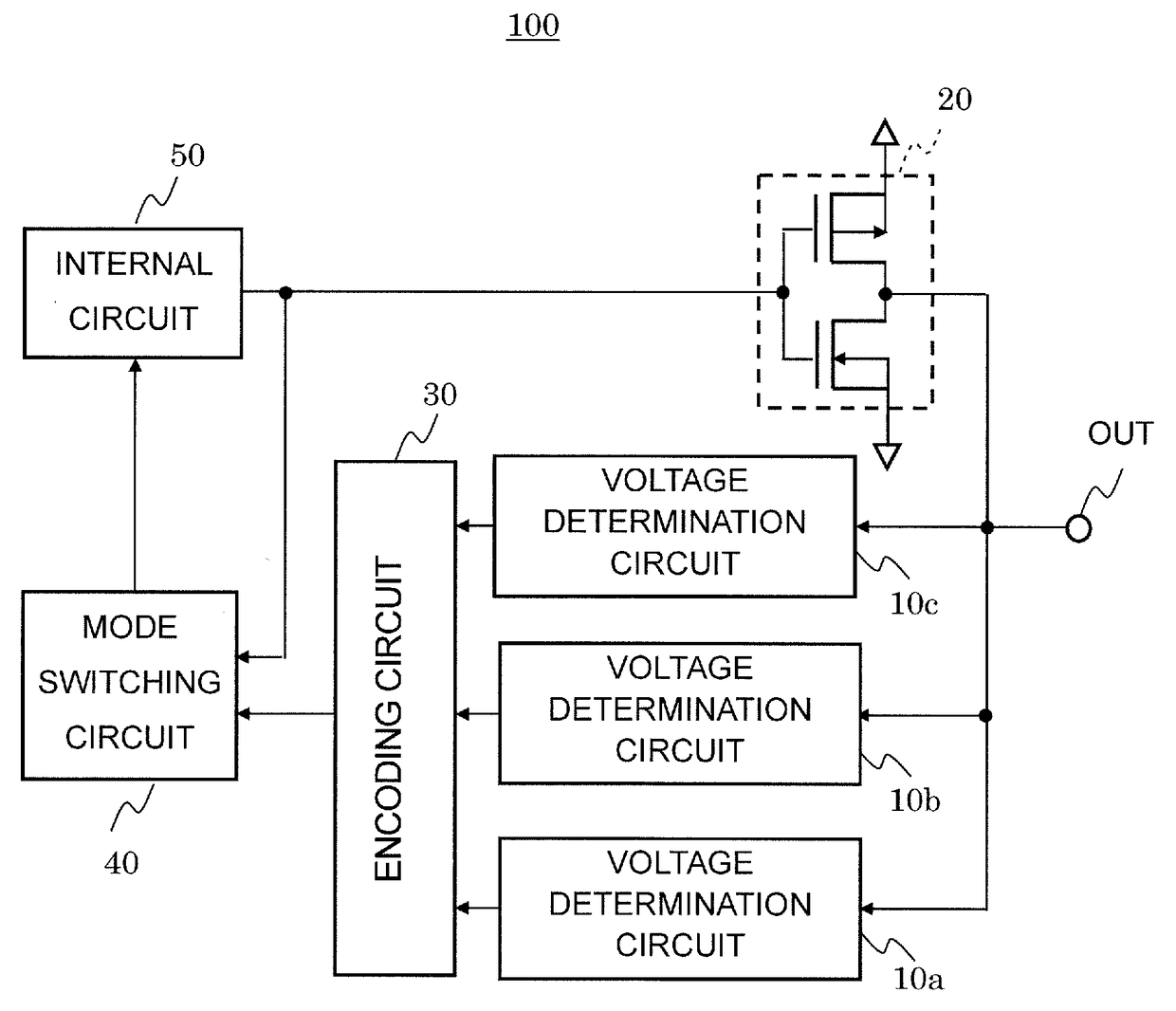
[0013]FIG. 1 is a block diagram of a semiconductor device 100 according to a first embodiment of the present invention.
[0014]The semiconductor device 100 according to the first embodiment includes voltage determination circuits 10a, 10b, and 10c, an output driver 20, an encoding circuit 30, a mode switching circuit 40, and an internal circuit 50.
[0015]The output driver 20 has an input connected to an output of the internal circuit 50, and an output connected to an output terminal OUT of the semiconductor device 100. The output terminal OUT is connected to inputs of the voltage determination circuits 10a, 10b, and 10c. The voltage determination circuits 10a, 10b, and 10c have outputs connected to inputs of the encoding circuit 30, respectively. The encoding circuit 30 has an output connected to a first input of the mode switching circuit 40. The mode switching circuit 40 has a second input connected to the output of the internal circuit 50, and an output connected to an input of the ...
second embodiment
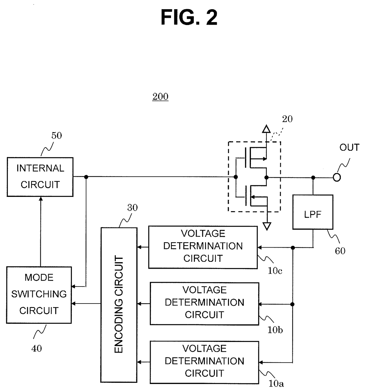
[0038]FIG. 2 is a block diagram of a semiconductor device 200 according to a second embodiment of the present invention. The semiconductor device 200 according to the second embodiment includes a low-pass filter 60 in addition to the semiconductor device 100 of FIG. 1. The remaining configuration is the same as that of the semiconductor device 100 of FIG. 1. The same components are denoted by the same reference symbols and description thereof is omitted.
[0039]The low-pass filter 60 is connected between the output terminal OUT and the voltage determination circuits 10a to 10c. The low-pass filter 60 has a function of preventing, when pulsed noise is superimposed on the output terminal OUT, the potential VOUT of the output terminal OUT, which is input to the voltage determination circuits 10a to 10c, from being fluctuated by the noise.
[0040]When the internal circuit 50 outputs the H-level signal, the NMOS transistor of the output driver 20 is turned on, and the potential VOUT of the o...
third embodiment
[0044]FIG. 3 is a block diagram of a semiconductor device 300 according to a third embodiment of the present invention. The semiconductor device 300 according to the third embodiment further includes voltage determination circuits 10d and 10e, and an encoding circuit 31 in addition to the semiconductor device 100 of FIG. 1. The remaining configuration is the same as that of the semiconductor device 100 of FIG. 1. The same components are denoted by the same reference symbols and description thereof is omitted.
[0045]The voltage determination circuit 10d has a threshold value Vt4, and outputs an output signal V10d. The output signal V10d from the voltage determination circuit 10d becomes an H level when the potential VOUT of the output terminal OUT is the threshold value Vt4 or more, and becomes an L level when the potential VOUT of the output terminal OUT is less than the threshold value Vt4.
[0046]The voltage determination circuit 10e has a threshold value Vt5, and outputs an output s...
PUM
 Abstract
Description
Claims
Application Information
 - R&D Engineer
- R&D Manager
- IP Professional
- Industry Leading Data Capabilities
- Powerful AI technology
- Patent DNA Extraction
Browse by: Latest US Patents, China's latest patents, Technical Efficacy Thesaurus, Application Domain, Technology Topic, Popular Technical Reports.
© 2024 PatSnap. All rights reserved.Legal|Privacy policy|Modern Slavery Act Transparency Statement|Sitemap|About US| Contact US: help@patsnap.com