

Substrate processing method, substrate processing system and substrate processing apparatus
Active Publication Date: 2018-03-15
TOKYO ELECTRON LTD
View PDF0 Cites 0 Cited by
- Summary
- Abstract
- Description
- Claims
- Application Information
AI Technical Summary
Benefits of technology
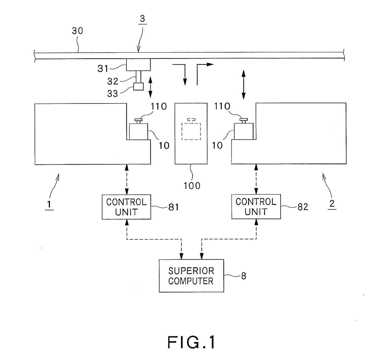
[0016]A substrate processing apparatus that applies a resist (first substrate processing apparatus) and a substrate processing apparatus that develops a substrate (second substrate processing apparatus) are separated from each other. A substrate having been heated after a resist coating process in the first substrate processing apparatus is also heated before an exposure process in the second substrate processing apparatus. Thus, even when amine in an atmosphere adheres to the processed substrate while the substrate is being transported by a carrier from the first substrate processing apparatus to the second substrate processing apparatus, the substrate is exposed and developed under the conditio
Problems solved by technology
When such a processing liquid adheres to the coating module, it is difficult to be removed.
Thus, as compared with an exp
Method used
View moreImage
Smart ImageViewing Examples

Examples
 PUM
 Abstract
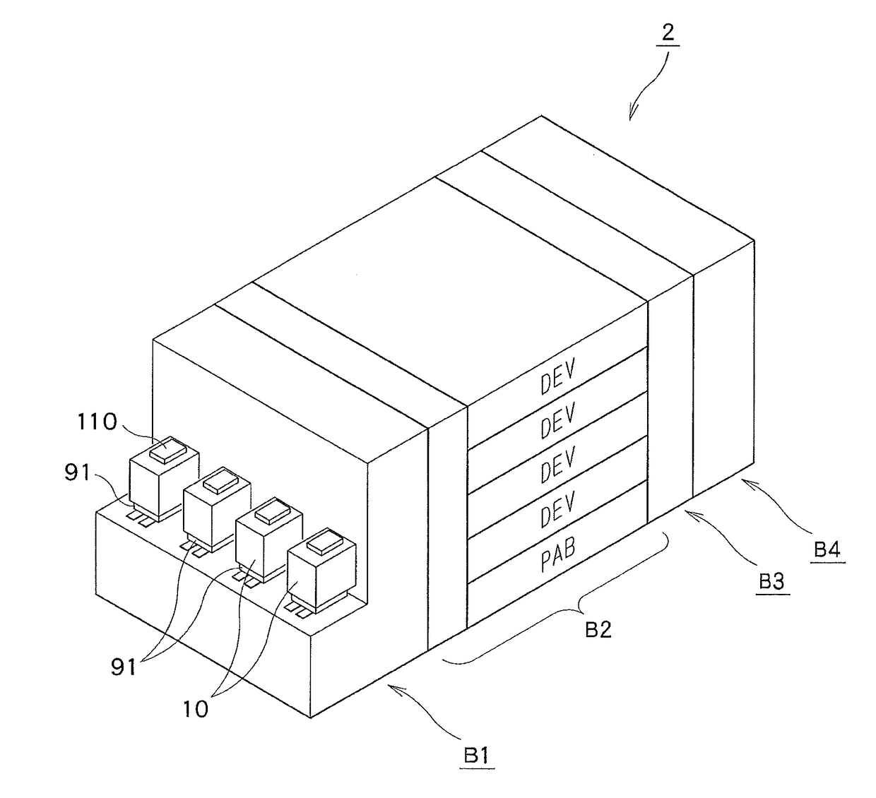
A technique enabling a stable resist pattern forming process, when substrate processing apparatuses that perform a resist coating process separately from a developing process. A wafer having been heated after a resist coating process in a first substrate processing apparatus is also heated before an exposure process in a second substrate processing apparatus. Thus, even when amine in an atmosphere adheres to the wafer while it is being transported from the first substrate processing apparatus to the second substrate processing apparatus, the amine scatters by the heating process. At least one of a heating time and a heating temperature is adjusted based on a substrate rest time which includes a period of time between a time point at which a FOUP 10 is unloaded from the first substrate processing apparatus and a time point at which the FOUP 10 is loaded into the second substrate processing apparatus.
Description
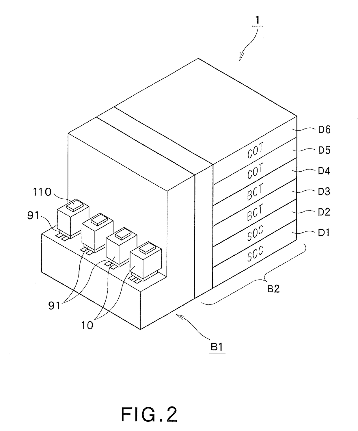
TECHNICAL FIELD[0001]The present invention relates to a technique for making uniform line widths of a resist pattern formed on a surface of a substrate.BACKGROUND ART[0002]In a photoresist step that is one of semiconductor manufacturing steps, a coating process in which a surface of a semiconductor wafer (referred to as “wafer” herebelow) is coated with various coating liquids such as a resist and so on, an exposure process in which a coating film is exposed, and a developing process in which the coating film is developed are performed so that a resist pattern is formed.[0003]In a substrate processing system in which the coating process and the developing process are performed, a processing liquid such as a resist liquid used in a coating module for applying a coating liquid is likely to solidify and adhere. When such a processing liquid adheres to the coating module, it is difficult to be removed. Thus, as compared with an exposure apparatus and a developing module, it takes longer...
Claims
Login to View More Application Information
Patent Timeline
 IPC IPC(8): H01L21/67H01L21/677G03F7/20
CPCH01L21/67225H01L21/67727H01L21/67733G03F7/70558G03F7/7075G03F7/70625G03F7/70875G03F7/70991H01L21/67109H01L21/6715H01L21/67253H01L21/67745H01L21/67748H01L21/68742G03F7/38G03F7/168G03F7/70483H01L21/027
InventorENOMOTO, MASASHIKONDO, YOSHIHIRO
OwnerTOKYO ELECTRON LTD