Manufacturing method of semiconductor device

a manufacturing method and semiconductor technology, applied in semiconductor/solid-state device manufacturing, basic electric elements, electric devices, etc., can solve the problems of unstable shape of the removal preventing film formed on the side wall at the time of etching, and achieve the effect of reducing the above variation and high accuracy

Inactive Publication Date: 2007-08-23
PANASONIC CORP
View PDF2 Cites 0 Cited by
  • Summary
  • Abstract
  • Description
  • Claims
  • Application Information

AI Technical Summary

Benefits of technology

[0009] Thus, it is an object of the present invention to reduce the above variation by c...

Problems solved by technology

As factors of the above variation in projection amount and round amount, it is cited that the shape of the removal preventing film formed on the side wall at the time of etc...

Method used


Image

  • Manufacturing method of semiconductor device
  • Manufacturing method of semiconductor device
  • Manufacturing method of semiconductor device

Examples


first embodiment

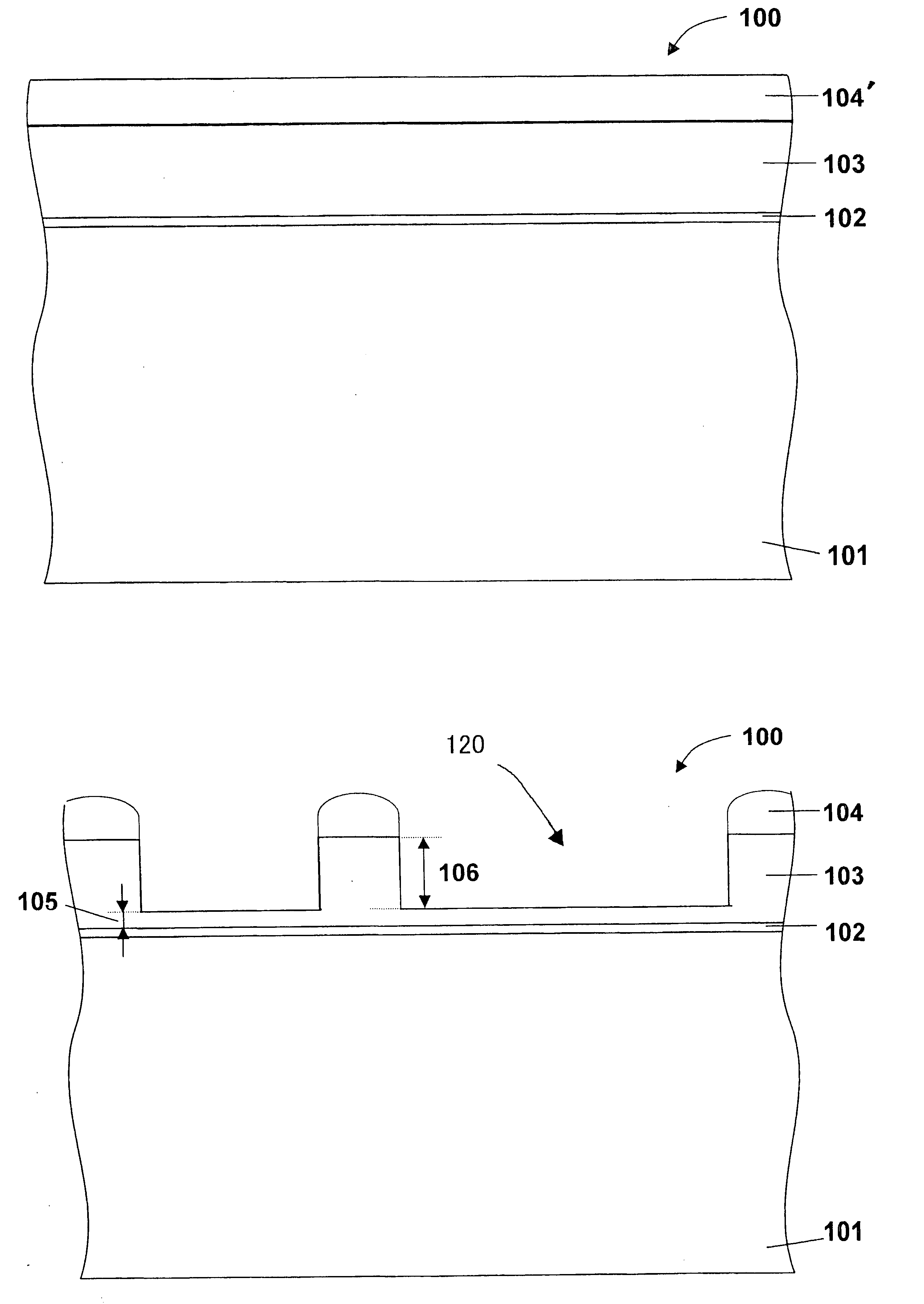
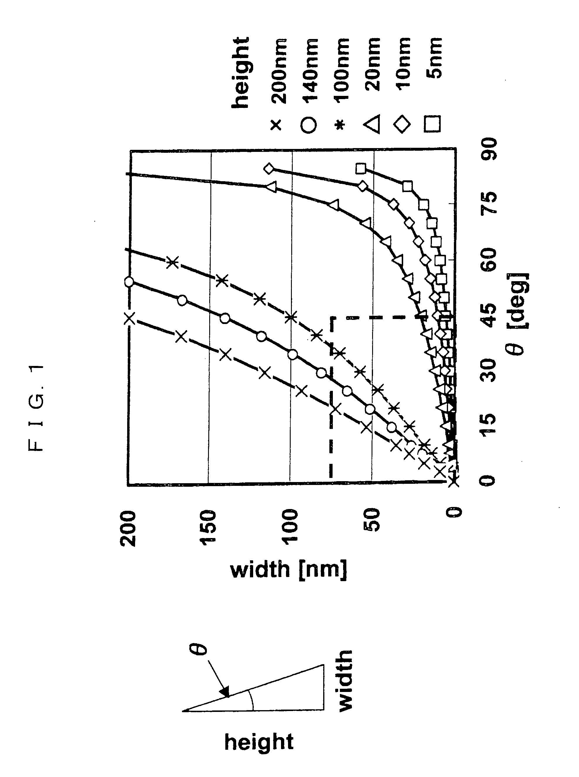
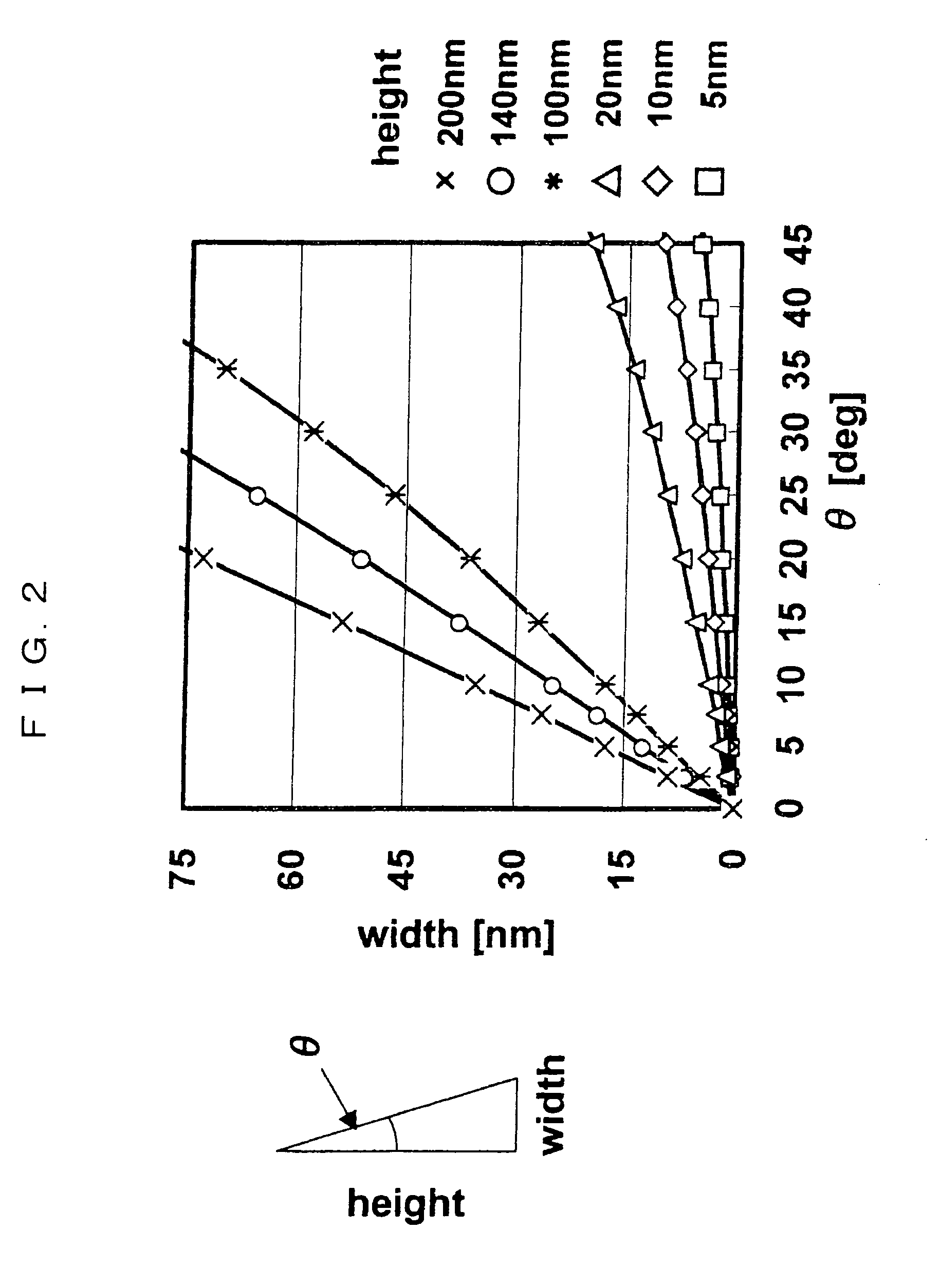
[0076] The first embodiment will be described with reference to FIGS. 3 to 8. First, at a step 1 shown in FIG. 3, a silicon oxide film (first film) 102 having thickness of 8 nm to 20 nm is formed on a p-type single-crystal silicon substrate (semiconductor substrate) 101 in a chamber atmosphere 100 by a thermal oxidation method. Then, a silicon nitride film (second film) 103 having thickness of 100 to 200 nm is deposited on the silicon oxide film 102 by a CVD method (vacuum pressure CVD method, plasma CVD method, high-density plasma CVD method, normal-pressure CVD method, or atomic layer deposition CVD method). Then, a photosensitive film (resist film) is coated onto the silicon nitride film 103 and performs patterning at exposing and developing steps to form a resist 104′ that defines an element isolation region. At this time, in order to reduce reflected light at the time of lithography, a reflection reducing film may be deposited between the silicon nitride film 103 and the photos...

second embodiment

[0093] A second embodiment of the present invention will be described with reference to FIGS. 9 and 10. In addition, in FIGS. 9 and 10, the reference numeral 200 designates a chamber atmosphere, the reference numeral 201 designates a silicon substrate, the reference numeral 202 designates a silicon oxide film, the reference numeral 203 designates a silicon nitride film, the reference numeral 203a designates a projecting part of the silicon nitride film 203, the reference numeral 204 designates a resist pattern, the reference numeral 205 designates a residual film of the silicon nitride film 203, the reference numeral 206 designates an etching amount of the silicon nitride film 203, the reference numerals 209 and 211 designate projection amounts of the projecting part 203a, the reference numeral 217 designates a second removal preventing film, the reference numeral 212 designates a taper angle of the second removal preventing film 217, the reference numeral 220 designates an opening,...

third embodiment

[0106] A third embodiment of the present invention will be described with reference to FIGS. 12 to 17. In addition, in FIGS. 12 to 17, the reference numeral 300 designates a chamber atmosphere, the reference numeral 301 designates a silicon substrate, the reference numeral 302 designates a silicon oxide film, the reference numeral 303 designates a silicon nitride film, and the reference numeral 304 designates a resist pattern.

[0107] A step 1 shown in FIG. 12 is similar to the step 1 (FIG. 3) in the first embodiment. Then, in step 2 shown in FIG. 13, a resist pattern 304 is formed so as to correspond to an element isolation region using a photolithography technique and then, the silicon nitride film 303 is etched away by anisotropic etching using the resist pattern 304 as a mask to form an opening in the silicon nitride film 303. In a step for etching the silicon nitride film 303, dry etching is performed using a mixture gas of CHF3 / CF4 / Ar / O2 until the silicon oxide film 302 of the ...


PUM


Abstract

A first film and a second film are formed on a semiconductor substrate in this order. A resist pattern is formed on the second film. An opening is formed by removing the second film exposed between the resist pattern at a state where the second film remains on the bottom. A first removal preventing film is formed on the side wall of the opening and the residual film is removed at a state where the projecting part of the second film protruding from the sidewall to the opening remains. The first film exposed in the opening is removed. A second removal preventing film is formed on the first removal preventing film and the surface of the semiconductor substrate exposed in the opening is removed at a state where the projecting part of the semiconductor substrate protruding from the side wall to the opening remains and a round part is formed at the projecting part of the semiconductor substrate. The semiconductor substrate exposed in the opening is further removed.

Description

BACKGROUND OF THE INVENTION [0001] 1. Field of the Invention [0002] The present invention relates to a manufacturing method of a semiconductor device and more particularly, to a method of forming a trench isolation for isolating elements. [0003] 2. Description of the Related Art [0004] Based on miniaturization of the semiconductor device, a shallow trench isolation (referred to as the STI hereinafter) in which a shallow trench is formed to bury an insulation film for element isolation has been widely used as a method of electrically isolating elements of sub-quarter micron devices. A conventional manufacturing method of a semiconductor device disclosed in U.S. Pat. No. 6,287,974 where shallow trench isolation is implemented will be described with reference to FIGS. 21 and 22. [0005] In FIGS. 21 and 22, the semiconductor device includes a chamber atmosphere 500, a silicon substrate 501, a silicon oxide film 502, a silicon nitride film 503, a resist pattern 504, the thickness of the s...

Claims


Application Information

Patent Timeline
IPC IPC(8): H01L21/84H01L21/00
CPCH01L21/76232
Inventor YAMADA, MASARUTSUDUMITANI, AKIHIKO
Owner PANASONIC CORP
Why Eureka
Try Eureka