

Semiconductor device and method for producing semiconductor device
- Summary
- Abstract
- Description
- Claims
- Application Information
AI Technical Summary
Benefits of technology
Problems solved by technology
Method used
Image

Examples
Embodiment Construction
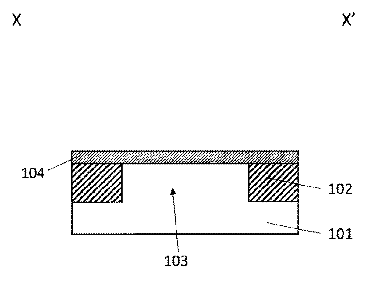
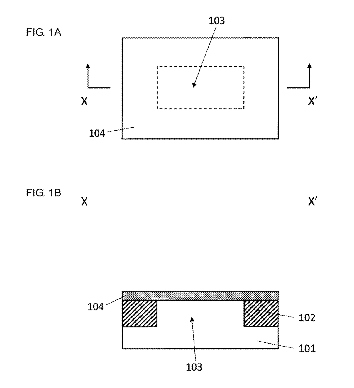
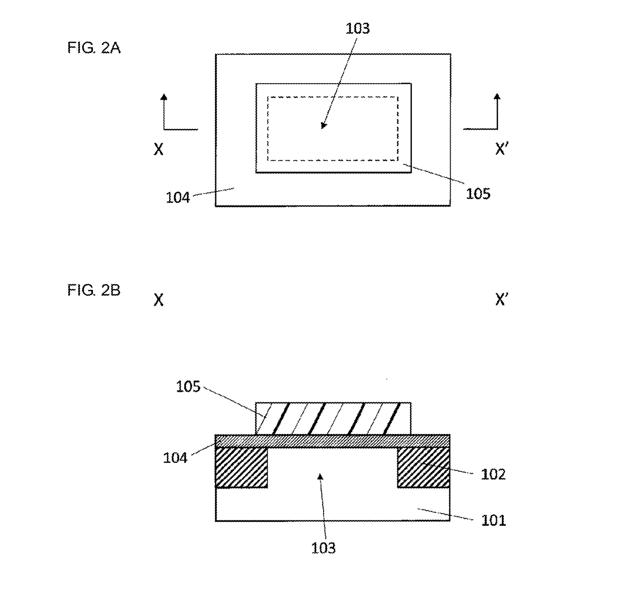
[0043]Hereinafter, a semiconductor device according to an embodiment of the present invention will be described with reference to FIGS. 21A and 21B. The semiconductor layer according to this embodiment is preferably a silicon layer. The semiconductor layer may be formed of another group IV semiconductor such as SiGe, Ge, or C. Alternatively, the semiconductor layer may be formed of a III-IV compound semiconductor.
[0044]The semiconductor device includes a planar semiconductor layer 103 formed on a substrate 101; a pillar-shaped semiconductor layer 114 formed on the planar semiconductor layer 103; a gate insulating film 113 surrounding the pillar-shaped semiconductor layer 114; a first metal 104 surrounding the gate insulating film 113, the first metal 104 being in contact with an upper portion of the planar semiconductor layer 103; a gate 107 formed above the first metal 104 so as to surround the gate insulating film 113, the gate 107 being electrically insulated from the first metal...
PUM
 Abstract
Description
Claims
Application Information