Method of producing semiconductor epitaxial wafer, semiconductor epitaxial wafer, and method of producing solid-state image sensing device

a semiconductor and epitaxial technology, applied in the direction of semiconductor devices, electrical equipment, radio frequency controlled devices, etc., can solve the problems of deteriorating the characteristics of semiconductor devices, increasing dark, and metal contamination, so as to reduce the damage of crystals, suppress metal contamination, and achieve the effect of high gettering capability

Active Publication Date: 2016-11-15
SUMCO CORP
View PDF18 Cites 0 Cited by
  • Summary
  • Abstract
  • Description
  • Claims
  • Application Information

AI Technical Summary

Benefits of technology

[0027]According to the method of producing a semiconductor wafer of the present invention, a semiconductor wafer is irradiated with cluster ions, and a modifying layer is formed from (a) constituent element(s) of the cluster ions in a surface portion of the semiconductor wafer, which allows the modifying layer to achieve higher gettering capability. Thus, a semiconductor epitaxial wafer which makes it possible to suppress metal contamination can be produced. Further, the irradiation with cluster ions can reduce damage to crystals as compared with single-ion implantation, which makes it possible to omit recovery heat treatment performed after the ion irradiation. Thus, the semiconductor epitaxial wafer can be more sufficiently produced.

Problems solved by technology

Metal contamination is one of the factors that deteriorate the characteristics of a semiconductor device.
For example, for a back-illuminated solid-state image sensing device, metal mixed into a semiconductor epitaxial wafer to be a substrate of the device causes increased dark current in the solid-state image sensing device, and results in formation of defects referred to as white spot defects.
In recent years, such metal contaminations have been reduced to some extent by replacing components of epitaxial growth furnaces with highly corrosion resistant materials, but not to a sufficient extent.
On the other hand, in the latter process of producing a solid-state image sensing device, heavy metal contamination of semiconductor substrates would occur in process steps such as ion implantation, diffusion, and oxidizing heat treatment in the producing process.

Method used


Image

  • Method of producing semiconductor epitaxial wafer, semiconductor epitaxial wafer, and method of producing solid-state image sensing device
  • Method of producing semiconductor epitaxial wafer, semiconductor epitaxial wafer, and method of producing solid-state image sensing device
  • Method of producing semiconductor epitaxial wafer, semiconductor epitaxial wafer, and method of producing solid-state image sensing device

Examples


experimental example 1

Example 1-1

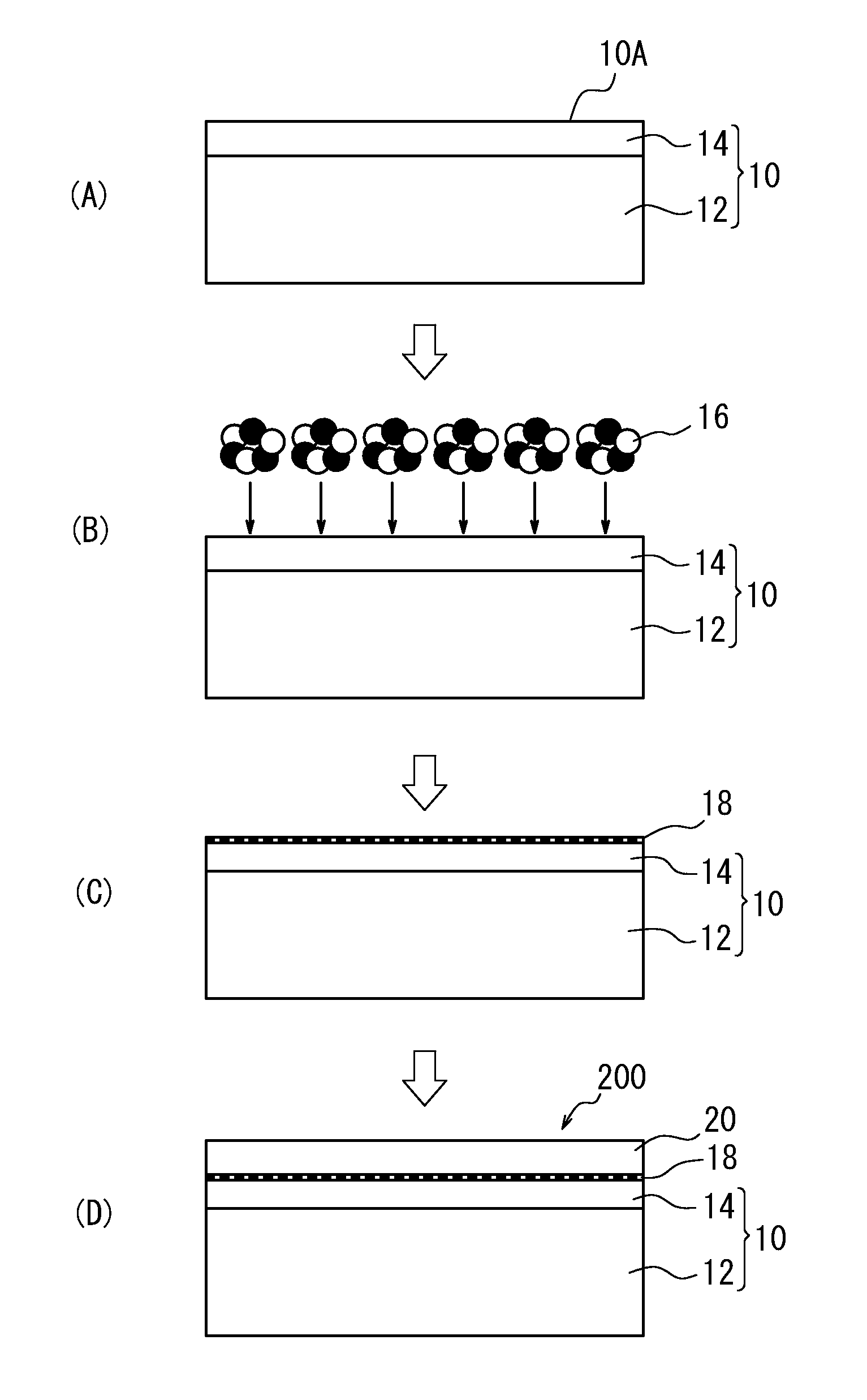
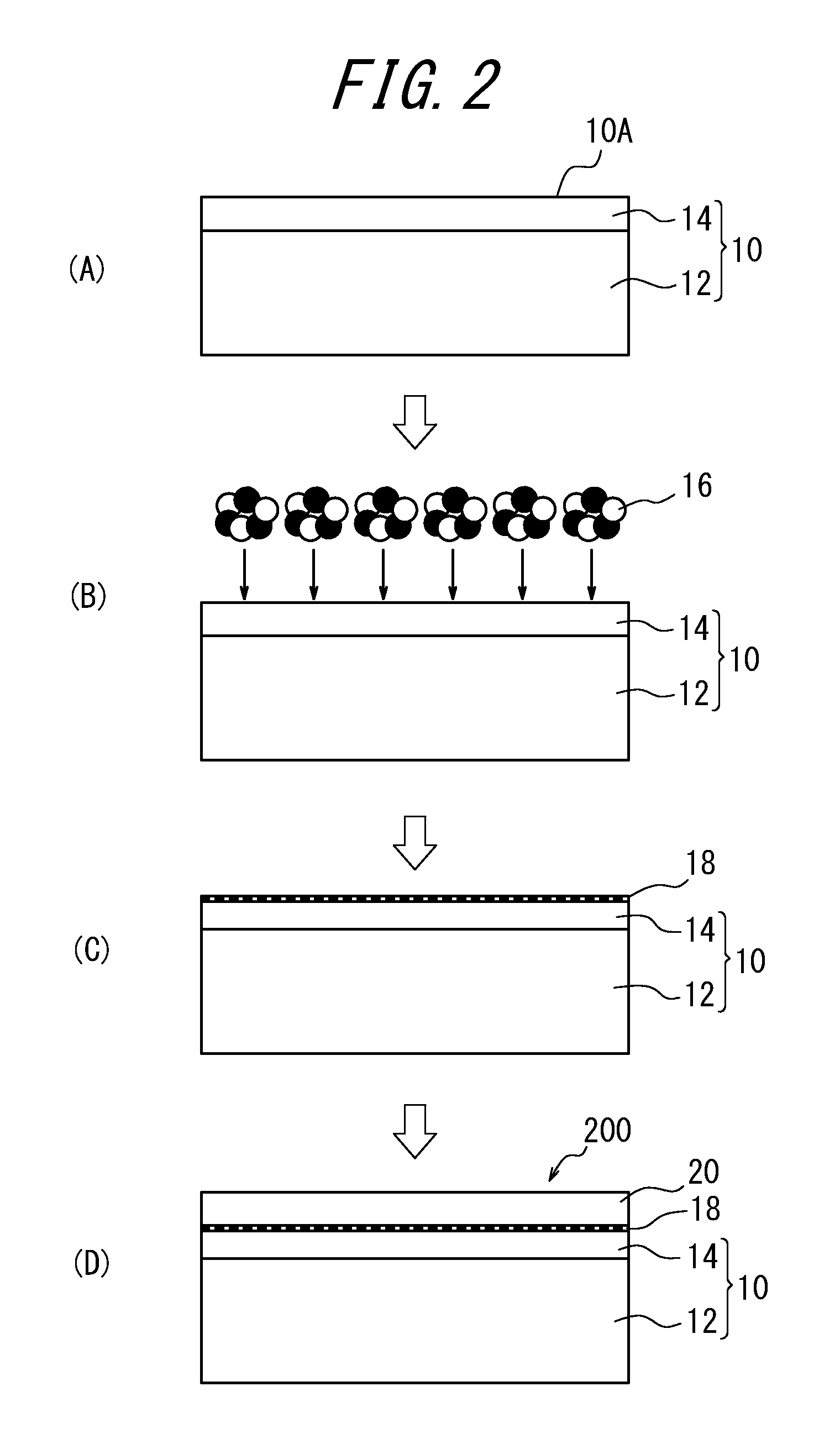
[0071]An n-type silicon wafer (thickness: 725 μm, kind of dopant: phosphorus, dopant concentration: 1×10¹⁵ atoms / cm3) obtained from a CZ crystal was prepared. Next, cluster ions were generated using a cluster ion generator (CLARIS produced by Nissin Ion Equipment Co., Ltd.) under the conditions shown in Table 1, and the silicon wafer was irradiated with the cluster ions. After that, recovery heat treatment under the conditions shown in Table 1 was performed using an RTA apparatus (produced by Mattson Thermal Products GmbH) as a heat treatment sufficient for recovering the crystallinity disrupted by the irradiation with cluster ions. Subsequently, the silicon wafer was transferred into a single wafer processing epitaxial growth apparatus (produced by Applied Materials, Inc.) and subjected to hydrogen baking at 1120° C. for 30 s in the apparatus. A silicon epitaxial layer (thickness: 4 μm, kind of dopant: phosphorus, dopant concentration: 1×10¹⁵ atoms / cm3) was then epitaxia...

examples 1-2 to 1-4

[0072]Silicon epitaxial wafers in accordance with the present invention were prepared in the same manner as Example 1-1 except that the cluster ion irradiation conditions and the recovery heat treatment conditions were changed as shown in Table 1. In Examples 1-2 and 1-4, recovery heat treatment using an RTA apparatus was not performed. The irradiation with cluster ions was performed at 80 keV / Cluster in Examples 1-1 to 1-4. The clusters each include three carbon atoms (atomic weight: 12) and three hydrogen atoms (atomic weight: 1). Therefore, the energy received by one carbon atom was 80×{12×3 / (12×3+1×3)} / 3=24.6 keV.

experimental example 2

Example 2-1

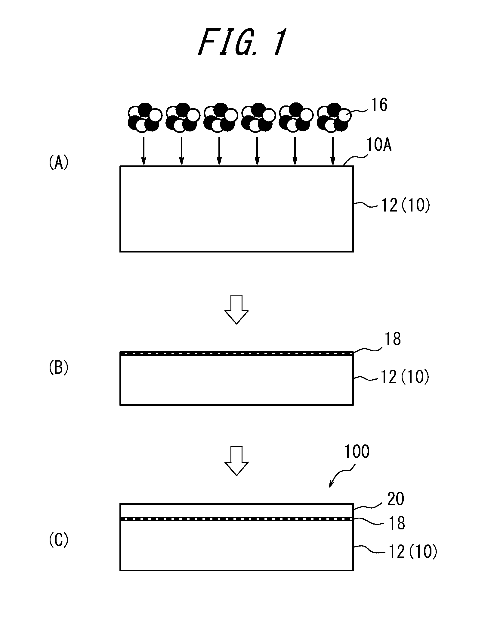
[0083]An n-type silicon wafer (thickness: 725 μm, kind of dopant: phosphorus, dopant concentration: 1×10¹⁵ atoms / cm3) obtained from a CZ crystal was transferred into a single wafer processing epitaxial growth apparatus (produced by Applied Materials, Inc.) and subjected to hydrogen baking at 1120° C. for 30 s in the apparatus. A first epitaxial layer of silicon (thickness: 0.3 μm, kind of dopant: phosphorus, dopant concentration: 1×10¹⁵ atoms / cm3) was then epitaxially grown on the wafer by CVD at 1150° C. using hydrogen as a carrier gas and dichlorosilane as a source gas. Next, cluster ions were generated using a cluster ion generator (CLARIS produced by Nissin Ion Equipment Co., Ltd.) under the conditions shown in Table 2, and the first epitaxial layer was irradiated with the cluster ions. After that, recovery heat treatment under the conditions shown in Table 2 was performed using an RTA apparatus (produced by Mattson Thermal Products GmbH) as a heat treatment sufficien...


PUM


Abstract

The present invention provides a method of more efficiently producing a semiconductor epitaxial wafer, which can suppress metal contamination by achieving higher gettering capability.A method of producing a semiconductor epitaxial wafer 100 according to the present invention includes a first step of irradiating a semiconductor wafer 10 with cluster ions 16 to form a modifying layer 18 formed from a constituent element of the cluster ions 16 in a surface portion 10A of the semiconductor wafer; and a second step of forming an epitaxial layer 20 on the modifying layer 18 of the semiconductor wafer 10.

Description

TECHNICAL FIELD[0001]The present invention relates to a method of producing a semiconductor epitaxial wafer, a semiconductor epitaxial wafer, and a method of producing a solid-state image sensing device. The present invention particularly relates to a method of more efficiently producing a semiconductor epitaxial wafer, which can suppress metal contamination by achieving higher gettering capability.BACKGROUND ART[0002]Metal contamination is one of the factors that deteriorate the characteristics of a semiconductor device. For example, for a back-illuminated solid-state image sensing device, metal mixed into a semiconductor epitaxial wafer to be a substrate of the device causes increased dark current in the solid-state image sensing device, and results in formation of defects referred to as white spot defects. In recent years, back-illuminated solid-state image sensing devices have been widely used in digital video cameras and mobile phones such as smartphones, because they can direc...

Claims


Application Information

Patent Timeline
Patent Type & Authority Patents(United States)
IPC IPC(8): H01L21/02H01L29/36H01L27/146H01L21/265H01L21/322
CPCH01L21/02631H01L21/02381H01L21/02439H01L21/02532H01L21/02658H01L21/26566H01L21/3221H01L27/14687H01L29/36H01L27/1464H01L27/14698H01L21/3228H01L21/322H01L21/20H01L21/265H01L27/146
Inventor KADONO, TAKESHIKURITA, KAZUNARI
Owner SUMCO CORP
Why Eureka
Try Eureka