

Shift register circuit
a shift register and register circuit technology, applied in the field of shift register circuits, can solve the problems of malfunction of the shift register circuit, inability to control the on-off state of at least a part of the thin-film transistor, and inability to transmit video signals representing pixel voltage values for a plurality of rows, so as to prevent the occurrence of malfunction caused by a threshold shift of the voltage dividing transistor, and prevent the effect of positive bias
- Summary
- Abstract
- Description
- Claims
- Application Information
AI Technical Summary
Benefits of technology
Problems solved by technology
Method used
Image

Examples
first embodiment
1. First Embodiment
[0153]
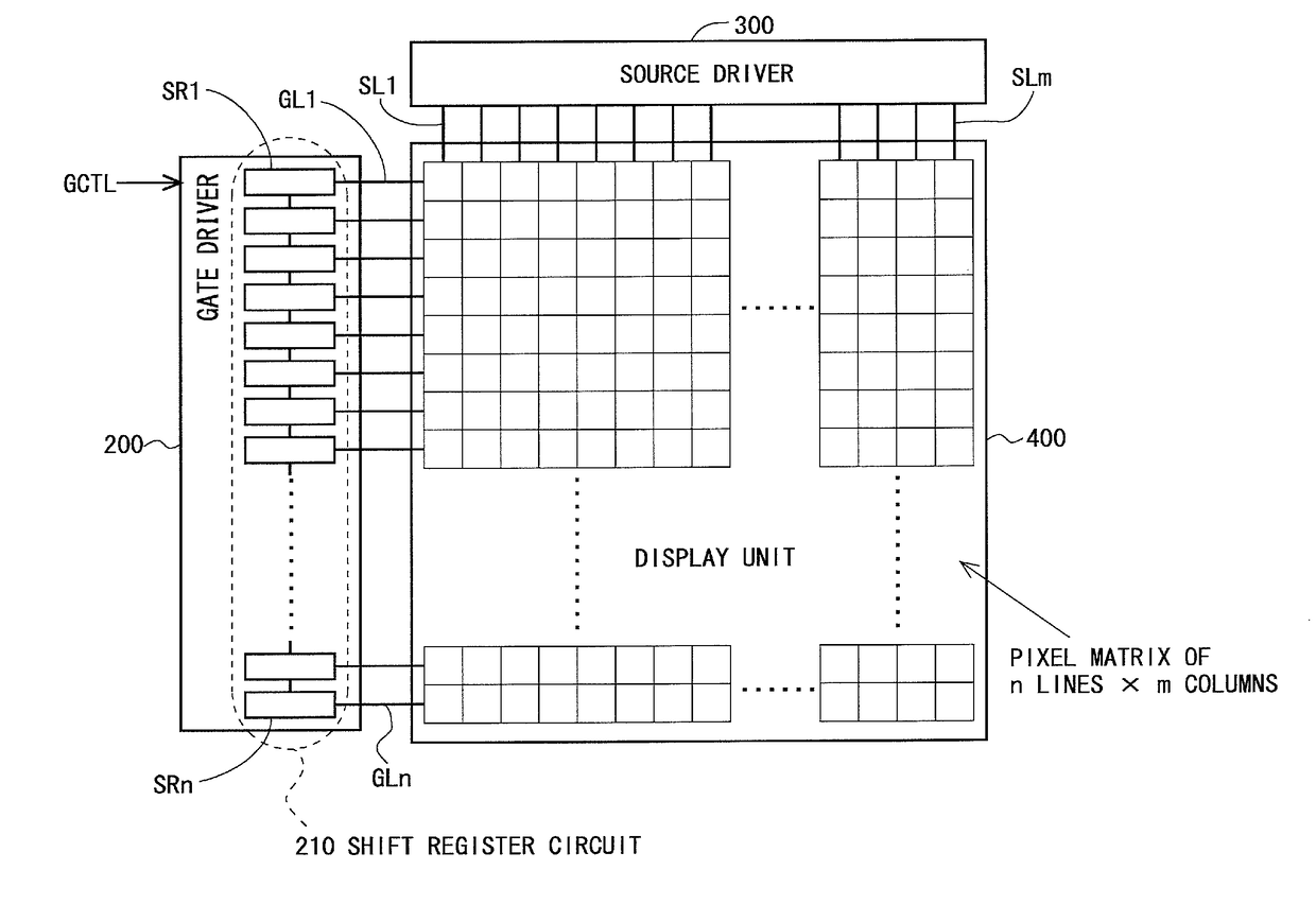
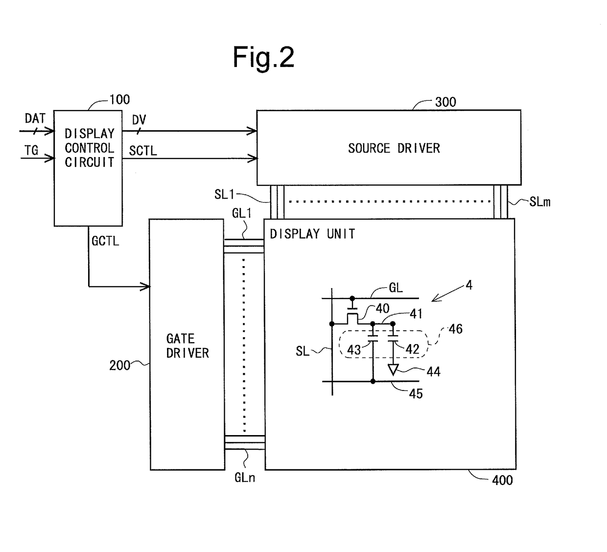
[0154]FIG. 2 is a block diagram showing an overall configuration of an active matrix-type liquid crystal display device according to a first embodiment of the present invention. As shown in FIG. 2, this liquid crystal display device includes a display control circuit 100, a gate driver (scanning signal line drive circuit) 200, a source driver (video signal line drive circuit) 300, and a display unit 400. It should be noted that the gate driver 200 is formed on a display panel including the display unit 400, using amorphous silicon, polycrystalline silicon, microcrystalline silicon, oxide semiconductor (e.g., indium gallium zinc oxide), or the like. In other words, in this embodiment, the gate driver 200 and the display unit 400 are formed on the same substrate (a TFT substrate which is one of two substrates that constitute a liquid crystal panel).
[0155]The display unit 400 is provided with a plurality of (m) source bus lines (video signal lines) SL1 to SLm a...
second embodiment
2. Second Embodiment
[0200]
[0201]A second embodiment of the present invention will be described. An overall configuration and a schematic configuration of the shift register circuit 210 are the same as those in the first embodiment, and shall not be described (see FIG. 2 to FIG. 4).
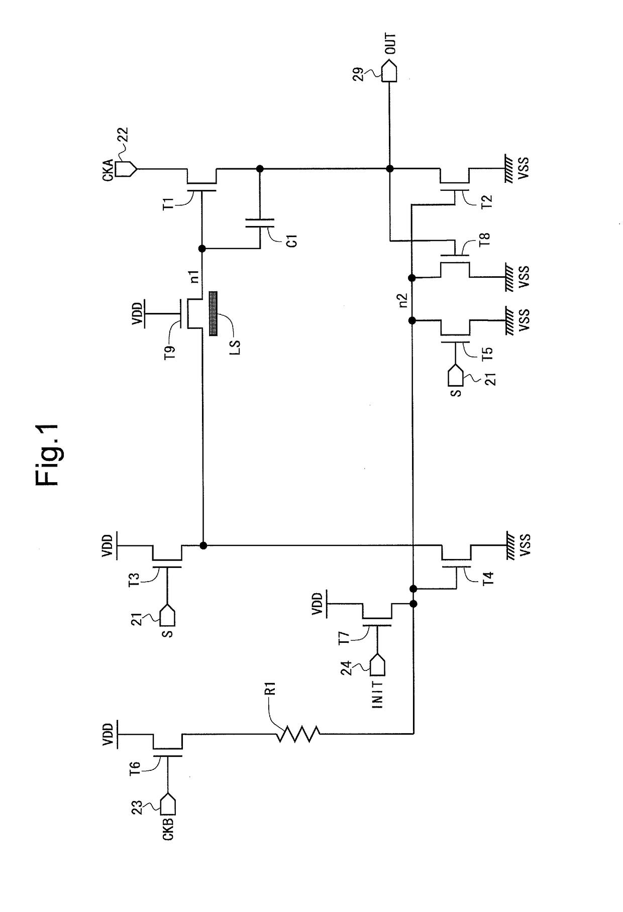
[0202]FIG. 7 is a circuit diagram showing a configuration of the unit circuit SR (configuration of a single stage of the shift register circuit 210) according to this embodiment. The unit circuit SR according to this embodiment is not provided with the thin-film transistor T9 that is provided for the unit circuit SR of the first embodiment (see FIG. 1). Therefore, in this embodiment, a region (wiring) where the gate terminal of the thin-film transistor T1, the source terminal of thin-film transistor T3, the drain terminal of the thin-film transistor T4, and the one end of the capacitor C1 are connected to each other is referred to as a “first node”. The first node is indicated by a reference symbol n1. Oth...
third embodiment
3. Third Embodiment
[0211]
[0212]A third embodiment of the present invention will be described. An overall configuration and a schematic configuration of the shift register circuit 210 are the same as the first embodiment, and shall not be described (see FIG. 2 to FIG. 4).
[0213]FIG. 10 is a circuit diagram showing a configuration of the unit circuit SR (configuration of a single stage of the shift register circuit 210) according to this embodiment. A circuit configuration of the unit circuit SR according to this embodiment is the same as the circuit configuration of the unit circuit SR according to the second embodiment. However, as can be seen from FIG. 7 and FIG. 10, while the light shielding film LS is only provided for the thin-film transistors T2 and T4 in the second embodiment, the light shielding film LS is only provided for the thin-film transistor T1 in this embodiment. It should be noted that an operation of the shift register circuit 210 is also the same as in the second em...
PUM
 Abstract
Description
Claims
Application Information