Semiconductor structure and a manufacturing method thereof

Inactive Publication Date: 2018-06-14
NAN YA TECH
View PDF9 Cites 1 Cited by
  • Summary
  • Abstract
  • Description
  • Claims
  • Application Information

AI Technical Summary

Benefits of technology

The present patent outlines a new invention and its features and benefits. The invention can be modified or designed for different purposes without changing its core purpose and scope. The technical effects of this patent are its broadly described features and benefits, which can be used as a basis for modifying or designing other structures or processes.

Problems solved by technology

The manufacturing of semiconductor devices using package on package is becoming more complicated.
Since many components with different materials are combined, the complexity of the manufacturing operations of the semiconductor device is increased.

Method used


Image

  • Semiconductor structure and a manufacturing method thereof
  • Semiconductor structure and a manufacturing method thereof
  • Semiconductor structure and a manufacturing method thereof

Examples


Embodiment Construction

[0035]The following description of the disclosure accompanies drawings, which are incorporated in and constitute a part of this specification, and illustrate embodiments of the disclosure, but the disclosure is not limited to the embodiments. In addition, the following embodiments can be properly integrated to complete another embodiment.

[0036]References to “one embodiment,”“an embodiment,”“exemplary embodiment,”“other embodiments,”“another embodiment,” etc. indicate that the embodiment(s) of the disclosure so described may include a particular feature, structure, or characteristic, but not every embodiment necessarily includes the particular feature, structure, or characteristic. Further, repeated use of the phrase “in the embodiment” does not necessarily refer to the same embodiment, although it may.

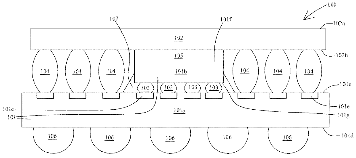
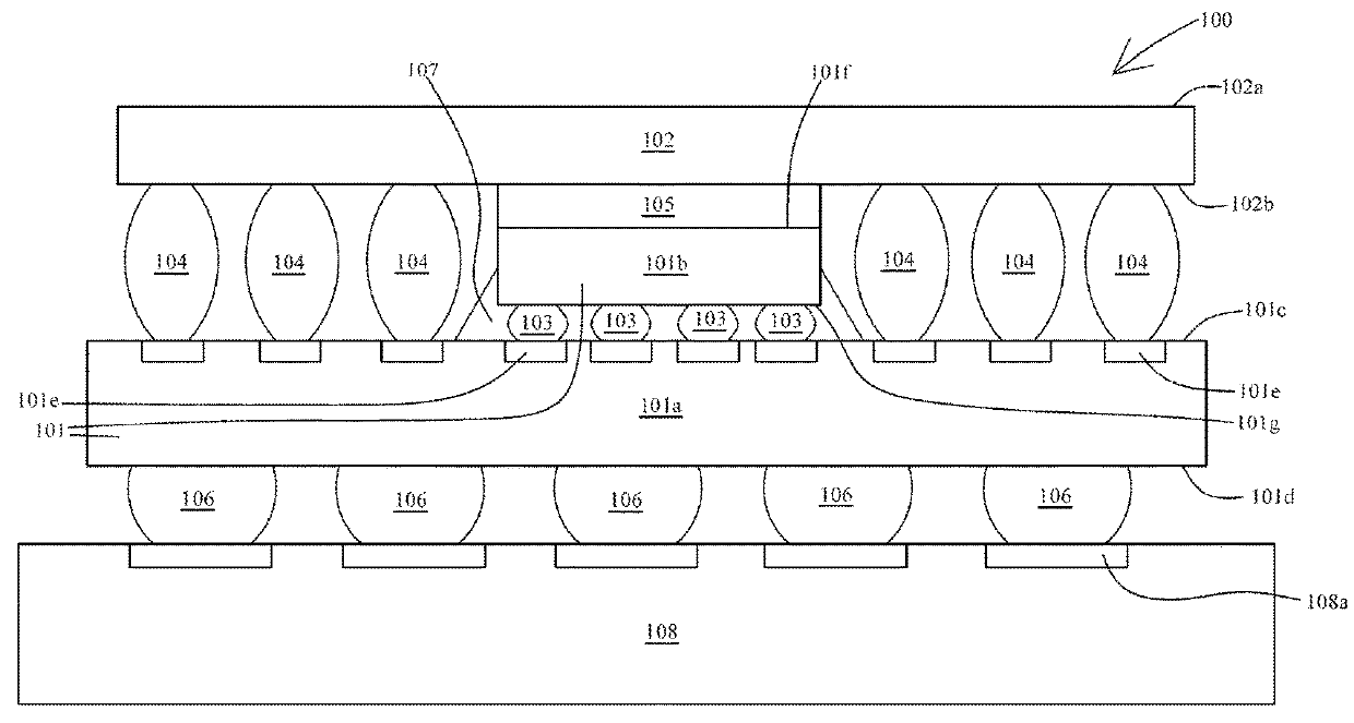
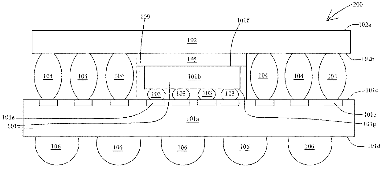
[0037]The present disclosure is directed to a semiconductor structure comprising an adhesive disposed between a first package and a second package. Also, the present disclosure is dire...


PUM


Abstract

A semiconductor structure includes a first package including a substrate and a die disposed over the substrate and electrically connected to the substrate by a first conductive bump; a second package disposed over the first package and electrically connected to the substrate by a second conductive bump; and an adhesive disposed between the die and the second package.

Description

TECHNICAL FIELD[0001]The present disclosure relates to a semiconductor structure, and particularly relates to a package on package (PoP) structure. A package is disposed over another package, and an adhesive is disposed between the packages. Further, a method of manufacturing a semiconductor structure comprises disposing an adhesive between packages.DISCUSSION OF THE BACKGROUND[0002]Semiconductor devices are essential for many modern applications. With the advancement of electronic technology, semiconductor devices are becoming smaller in size while having greater functionality and greater amounts of integrated circuitry. Due to the miniaturized scale of semiconductor devices, package on package (PoP) is now widely used for manufacturing. Numerous manufacturing steps are undertaken in the production of such packaging structure.[0003]The manufacturing of semiconductor devices using package on package is becoming more complicated. The semiconductor device is assembled with a number of...

Claims


Application Information

Patent Timeline
IPC IPC(8): H01L25/10H01L25/00H01L23/00H01L23/31H01L21/48H01L21/56
CPCH01L25/105H01L25/50H01L24/16H01L23/3185H01L2224/16227H01L21/563H01L2225/1023H01L2225/1058H01L2225/1094H01L21/4853H01L23/49816H01L24/32H01L24/81H01L24/83H01L2224/32238H01L2224/32227H01L2224/16238H01L2224/81H01L2224/83H01L23/562H01L2224/32225H01L2224/73204H01L2224/73253H01L2224/83191H01L2224/83192H01L2224/92125H01L2224/92225H01L2924/15311H01L2924/15331H01L2924/3511H01L24/17H01L2224/92242H01L2224/29324H01L24/05H01L24/11H01L24/13H01L24/29H01L24/33H01L24/73H01L24/92H01L2224/0391H01L2224/05164H01L2224/05184H01L2224/05624H01L2224/05639H01L2224/05644H01L2224/05647H01L2224/05655H01L2224/05664H01L2224/05684H01L2224/1132H01L2224/131H01L2224/13294H01L2224/133H01L2224/16145H01L2224/1703H01L2224/17181H01L2224/2929H01L2224/29339H01L2224/29393H01L2224/32145H01L2224/33181H01L2224/8112H01L2224/81424H01L2224/81439H01L2224/81444H01L2224/81447H01L2224/81455H01L2224/81464H01L2224/81815H01L2224/11515H01L2224/81484H01L2224/92222H01L2224/13147H01L2224/13155H01L2224/13144H01L2224/11334H01L2224/11849H01L2224/2919H01L2224/05147H01L2224/05139H01L2224/05144H01L2224/05124H01L2224/05155H01L2924/014H01L2224/27H01L2924/00014H01L2924/01006H01L2924/00H01L2224/16225H01L2924/0665
Inventor LIN, PO CHUN
Owner NAN YA TECH
Why Eureka
Try Eureka