Top-emitting OLED device and method of manufacturing the same, display device

a technology of display device and oled device, which is applied in the direction of semiconductor devices, organic semiconductor devices, electrical devices, etc., can solve the problems of narrowed visual angle, color difference of exiting light, and relatively complex manufacturing process, and achieve the effect of improving the display performance of the display devi

Inactive Publication Date: 2018-06-14
BOE TECH GRP CO LTD
View PDF3 Cites 18 Cited by
  • Summary
  • Abstract
  • Description
  • Claims
  • Application Information

AI Technical Summary

Benefits of technology

[0010]The present disclosure aims to provide a top-emitting organic light-emitting diode (OLED) device, a method of manufacturing the top-emitting OLED device and a display device comprising the top-emitting OLED device, which are capable of improving display performance of the display device.
[0012]The top-emitting OLED device according to the embodiment of the present disclosure can not only keep the microcavity effect, but also reduce the viewing angle dependence of the top-emitting OLED device, so that it can avoid color difference of exiting light and narrowed visual angle of the OLED device. Further, the OLED device according to the embodiment of the present disclosure can avoid the lateral light leakage of a display device comprising the OLED device.

Problems solved by technology

The microcavity effect will cause a luminescent spectrum of the OLED to be changed as a viewing angle changes so that the OLED device has viewing angle dependence, thereby leading to color difference of exiting light and narrowed visual angle.
However, as the DBR structure is generally formed by laminating a plurality of films having different refractive indexes alternately, it is required to control the film thickness strictly, so that the manufacturing process is relatively complex.
Moreover, the microcavity may have an advantage which enhances a front light-exiting efficiency of the device, this advantage may also be weakened as the microcavity effect is reduced.
An assembly formed by assembling the color film substrate and the above OLED has a large thickness, and light emitted from an edge of pixel of the OLED towards the color film substrate has a large exiting angle, which may cause light emitted from one pixel region of the OLED to be transmitted to the color film of adjacent pixel regions, thereby leading to lateral light leakage and thus abnormal display.

Method used


Image

  • Top-emitting OLED device and method of manufacturing the same, display device
  • Top-emitting OLED device and method of manufacturing the same, display device
  • Top-emitting OLED device and method of manufacturing the same, display device

Examples


Embodiment Construction

[0052]In the following detailed description, in order to facilitate the explanation, a number of specific details are explained to provide a comprehensive understanding to the embodiments of the present disclosure. However, it is obvious that one or more embodiments may be implemented without these specific details. In other cases, conventional structures and devices are shown in schematic diagrams to simplify the drawings. Moreover, the expression “disposed on” used in the specification may be meant that a component is disposed directly on another component, or that a component is disposed above another component and there is an intermediate component between the two components.

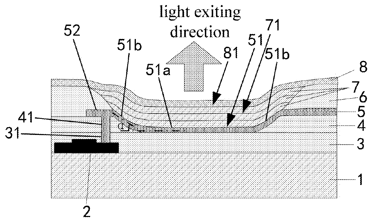
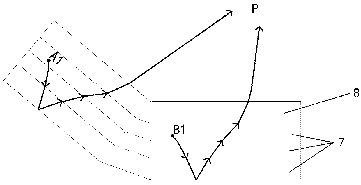
[0053]FIG. 1A is a partial sectional view of a top-emitting OLED device according to an embodiment of the present disclosure, and FIG. 1B is a schematic view showing exemplary paths through which light emitted from different points in the OLED device in FIG. 1A is projected to a view point.

[0054]As shown in ...


PUM


Abstract

A top-emitting OLED device includes: a substrate; a first electrode disposed on the substrate; an organic layer disposed on the first electrode; and a second electrode disposed on the organic layer, through which light emitted from the organic layer exits from the OLED device; wherein the first electrode comprises a curved structure recessed towards the substrate. The top-emitting OLED device can reduce the viewing angle dependence of the top-emitting OLED device, so that it can prevent color difference of exiting light, narrowed visual angle of the OLED device and lateral light leakage from occurring.

Description

CROSS-REFERENCE TO RELATED APPLICATION[0001]This application is a Section 371 National Stage Application of International Application No. PCT / CN2015 / 092305, filed on Oct. 20, 2015, entitled “TOP-EMITTING OLED DEVICE AND METHOD OF MANUFACTURING THE SAME, DISPLAY DEVICE”, which has not yet published, which claims priority to Chinese Application No. 201410569281.2, filed on Oct. 22, 2014, incorporated herein by reference in their entirety.BACKGROUND OF THE INVENTIONField of the Invention[0002]Embodiments of the present disclosure relate to a light-emitting device in a display device, in particular, to a top-emitting organic light-emitting diode (OLED) device, a method of manufacturing the top-emitting OLED device and a display device comprising the OLED device.Description of the Related Art[0003]An organic light-emitting diode (OLED) device has advantages, such as active light-emitting, good temperature characteristic, low power consumption, fast response speed, flexibility, ultra-thin...

Claims


Application Information

Patent Timeline
Patent Type & Authority Applications(United States)
IPC IPC(8): H01L51/52H01L51/56H01L51/00H01L27/32
CPCH01L51/5209H01L51/5218H01L51/56H01L51/001H01L27/3246H01L27/3258H01L2251/5315H01L2227/323H10K50/805H10K50/813H10K50/822H10K71/00H10K2102/3026H10K59/124H10K50/818H10K59/122H10K71/164H10K59/1201
Inventor DAI, QINGLIU, ZE
Owner BOE TECH GRP CO LTD
Why Eureka
Try Eureka