Flexible display device and manufacturing method thereof

a display device and flexible technology, applied in the direction of sustainable manufacturing/processing, instruments, final product manufacturing, etc., can solve the problems of low yield (proportion of output to input of goods), disadvantageous to realize the flexibility of a glass material sealing substrate, and inability to meet the needs of customers, etc., to achieve the effect of increasing manufacturing yield, thin thickness and large siz

Active Publication Date: 2018-06-28
SAMSUNG DISPLAY CO LTD
View PDF6 Cites 18 Cited by
  • Summary
  • Abstract
  • Description
  • Claims
  • Application Information

AI Technical Summary

Benefits of technology

[0007]According to an aspect of embodiments of the present invention, a large and thin flexible display device and a manufacturing method thereof may improve a sealing effect of a display part, without a sealing substrate made of a glass material, or a thin film encapsulation.
[0015]According to an aspect of the flexible display device according to one or more exemplary embodiments, it is possible to ensure sealing performance of a display part, to have a large size and a thin thickness, and increase a manufacturing yield.

Problems solved by technology

In a case of a large-sized flexible organic light emitting diode display device, it is difficult to realize flexibility of a sealing substrate made of a glass material, and it is disadvantageous to realize a display device to be thin.
The thin film encapsulation has excellent flexibility, but when it is applied to a long manufacturing process, a yield (proportion of output to input of goods) is low.

Method used


Image

  • Flexible display device and manufacturing method thereof
  • Flexible display device and manufacturing method thereof
  • Flexible display device and manufacturing method thereof

Examples


Embodiment Construction

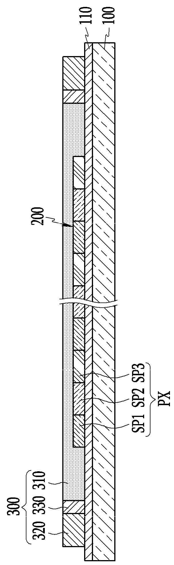
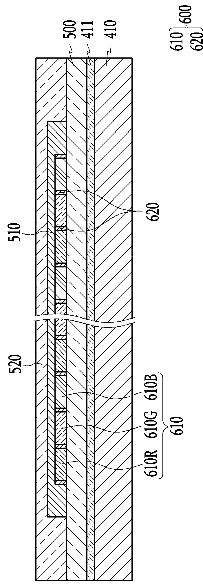
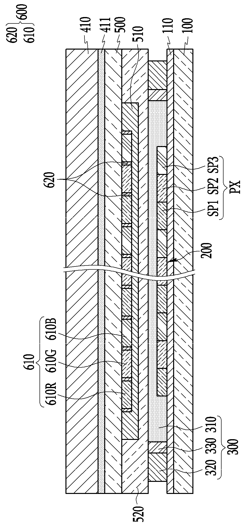
[0021]The present disclosure will be described more fully herein with reference to the accompanying drawings, in which some exemplary embodiments of the disclosure are shown. As those skilled in the art would realize, the described embodiments may be modified in various different ways, all without departing from the spirit or scope of the present disclosure.

[0022]To more clearly describe the present disclosure, portions which do not relate to the description may be omitted, and like reference numerals designate like elements throughout the specification.

[0023]Further, the size and thickness of each component shown in the drawings may be arbitrarily shown for better understanding and ease of description, but the present disclosure is not limited thereto. In the drawings, the thicknesses of layers, films, panels, regions, areas, etc., may be exaggerated for clarity.

[0024]It is to be understood that when an element, such as a layer, film, region, or substrate is referred to as being “o...


PUM


Abstract

A flexible display device includes: a first flexible substrate and a second flexible substrate facing each other; a display part positioned on a surface of the first flexible substrate facing the second flexible substrate and including a plurality of thin film transistors and a plurality of light emitting elements; a color filter positioned on a surface of the second flexible substrate facing the first flexible substrate; an overcoat layer positioned between the display part and the color filter and covering the color filter; a gas barrier layer positioned between the display part and the overcoat layer and covering the overcoat layer; and an encapsulation part including a filler positioned between the display part and the gas barrier layer, and a sealant positioned at an outside of the filler, and an area of the gas barrier layer is larger than an area of the encapsulation part.

Description

CROSS-REFERENCE TO RELATED APPLICATION[0001]This application claims priority to and the benefit of Korean Patent Application No. 10-2016-0177825, filed on Dec. 23, 2016 in the Korean Intellectual Property Office, the entire content of which is incorporated herein by reference.BACKGROUND1. Field[0002]Aspects of embodiments of the present disclosure relate to a flexible display device.2. Description of the Related Art[0003]A typical organic light emitting diode display device includes a substrate, a display part positioned on the substrate and including a plurality of thin film transistors and a plurality of organic light emitting diodes, and an encapsulation part that seals the display part to block moisture and oxygen included in outside air from penetrating thereto.[0004]In a case of a small-sized organic light emitting diode display device, the encapsulation part may be a thin film encapsulation in which a plurality of inorganic layers and a plurality of organic layers are alterna...

Claims


Application Information

Patent Timeline
Patent Type & Authority Applications(United States)
IPC IPC(8): H01L51/00H01L51/52H01L51/56
CPCH01L51/0097H01L51/5246H01L51/5259H01L51/5253H01L51/56G02B5/20H01L2251/5338G02B5/201Y02E10/549Y02P70/50H10K77/111H10K50/846H10K50/8426H10K50/844H10K2102/311H10K59/40H10K71/80H10K50/865H10K2102/00H10K71/00
Inventor LIM, HEUNG KYOONNAM, KIE HYUN
Owner SAMSUNG DISPLAY CO LTD
Why Eureka
Try Eureka