A goa circuit and a liquid crystal display

a liquid crystal display and circuit technology, applied in the field of liquid crystal display technology, can solve problems such as failure of goa circui

Active Publication Date: 2018-07-26
SHENZHEN CHINA STAR OPTOELECTRONICS TECH CO LTD
View PDF2 Cites 2 Cited by
  • Summary
  • Abstract
  • Description
  • Claims
  • Application Information

AI Technical Summary

Benefits of technology

[0025]The present application has the advantages, comparing to the conventional technology, the GOA circuit of the present application includes a pull-up circuit including a first switching transistor, a pull-down circuit including a second switching transistor, a scanning output terminal coupled to the second connecting terminal of the first switching transistor, and a first connecting terminal of the second switching transistor; a clamping circuit coupling to the second connecting terminals of the first switching transistor and the second switching transistor, and coupling to the control terminals of the first switching transistor and the second switching transistor, when the scanning output terminal outputting a first electric level, controlling the electric level of the contr

Problems solved by technology

However, the turn-on voltage Vth of the thin-film transistor fabricated by I

Method used


Image

  • A goa circuit and a liquid crystal display
  • A goa circuit and a liquid crystal display
  • A goa circuit and a liquid crystal display

Examples


first embodiment

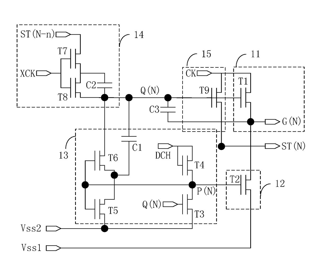
[0036]Referring to FIG. 1 is a schematic structural view of a GOA circuit according to the present application, the GOA circuit includes:

[0037]A pull-up circuit 11, includes a first switching transistor T1.

[0038]A pull-down circuit 12, includes a second switching transistor T2.

[0039]The scanning output terminal G(N) is coupled between a second connecting terminal of the first switching transistor T1 and a first connecting terminal of the second switching transistor T2.

[0040]Wherein, the first connecting terminal of the first switching transistor T1 is supplied with the first clock signal CK, and when a control terminal of the first switching transistor is at the high electric level, the first switching transistor T1 is turned on, and the first clock signal CK is outputted through the scanning output terminal G(N).

[0041]A clamping circuit 13: coupling the second connecting terminals of the first switching transistor T1 and the second switching transistor T2, and coupling the control ...

second embodiment

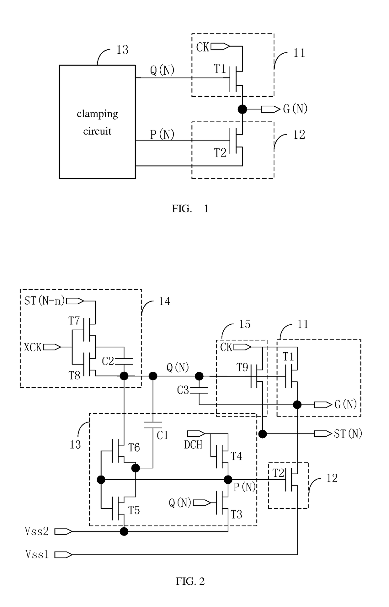
[0046]Referring to FIG. 2, FIG. 2 is a schematic diagram of a circuit connection according to the GOA circuit of the present application. The GOA circuit includes the pull-up circuit 11, the pull-down circuit 12, the clamping circuit 13, a pull-up control circuit 14, and a downstream circuit 15.

[0047]Wherein, the pull-up circuit 11 and the pull-down circuit 12 are the same as those of the first embodiment, and will not be described here.

[0048]Wherein the clamping circuit 13 includes:

[0049]The first clamp terminal Vss1, inputting the third electric level Vss1 and is coupled to the second connecting terminal of the second switching transistor T2.

[0050]The second clamp terminal Vss2, inputting the fourth electric level Vss2, and is coupled to the control terminal of the first switching transistor T1 through a control circuit and coupled to the control terminal of the second switching transistor T2; wherein the third electric level Vss1 is higher than the fourth electric level Vss2.

[005...

third embodiment

[0075]Referring to FIG. 5, FIG. 5 is a schematic diagram of a circuit connection according to the GOA circuit of the present application. The GOA circuit includes a pull-up circuit 11, a pull-down circuit 12, a clamping circuit 13, a pull-up control circuit 14, and a downstream circuit 15.

[0076]It should be noted that, the difference from the second embodiment is that the first capacitor C1 is removed from the GOA circuit of the present embodiment, the first connecting terminal of the eighth switching transistor T8 is coupled to the second connecting terminal of the sixth switching transistor T6. Such as the second capacitor C2 is also coupled to the first and second connecting terminals of the sixth switching transistor T6, so that a capacitance can be reduced, which facilitates the realization of the narrow border of the liquid crystal display.

[0077]It is to be understood that the connections of the other circuit elements of the present embodiment is the same as that of the above-...


PUM


Abstract

The present application discloses a GOA circuit and a liquid crystal display, the GOA circuit including: a pull-up circuit, including a first switching transistor; a pull-down circuit, including a second switching transistor; a scanning output terminal coupled to the second connecting terminal of the first switching transistor, and a first connecting terminal of the second switching transistor; and a clamping circuit, coupling to the second connecting terminals of the first switching transistor and the second switching transistor, and coupling to the control terminals of the first switching transistor and the second switching transistor, when the scanning output terminal outputting a first electric level, controlling the electric level of the control terminal of the second switching transistor lower than the electric level of the second connecting terminal of the second switching transistor. The present application prevents the transistor from erroneously turning on or off due to the turn on threshold shift.

Description

FIELD OF THE INVENTION[0001]The present application relates to a liquid crystal display technology field, and more particularly to a GOA circuit and a liquid crystal display.BACKGROUND OF THE INVENTION[0002]Gate Driver on Array, GOA technology can help to fabricate narrow border or borderless display products, and it can reduce the binding process for the external integrated circuit, IC, is conducive to enhance productivity and reduce product costs, which has been widely used and research.[0003]Indium Gallium Zinc Oxide, IGZO, because of its high mobility and good device stability, in the fabrication of GOA circuit, it can reduce the complexity of GOA circuit, has been widely used. In particular, because of its high mobility, when used in the fabrication of thin film transistors in GOA circuits, the size of the thin film transistor is smaller relative to the thin film transistor fabricated using amorphous silicon, a-Si, which is conducive to the production of narrow-border display; ...

Claims


Application Information

Patent Timeline
IPC IPC(8): G09G3/36G02F1/133
CPCG09G3/36G02F1/13306G09G2310/0264G09G3/3611G09G3/3677G09G2300/0408G09G3/3674
Inventor SHI, LONGQIANG
Owner SHENZHEN CHINA STAR OPTOELECTRONICS TECH CO LTD
Why Eureka
Try Eureka