Amoled display device and array substrate thereof

a technology which is applied in the field array substrate thereof, can solve the problems of low pixels per inch (ppi) and quantity of sub-pixel units and achieve the effect of improving the ppi of amoled display devi

Active Publication Date: 2018-08-02
SHENZHEN CHINA STAR OPTOELECTRONICS TECH CO LTD
View PDF5 Cites 6 Cited by
  • Summary
  • Abstract
  • Description
  • Claims
  • Application Information

AI Technical Summary

Benefits of technology

[0006]The present disclosure aims to provide an AMOLED display device and an array substrate thereof so as to improve PPI of the AMOLED display device.

Problems solved by technology

However, the mesh-shaped power lines occupy an over large layout space, which will limit a quantity of sub-pixel units, and lead to a low Pixels Per Inch (PPI) of the AMOLED display device.

Method used


Image

  • Amoled display device and array substrate thereof
  • Amoled display device and array substrate thereof
  • Amoled display device and array substrate thereof

Examples


embodiment 1

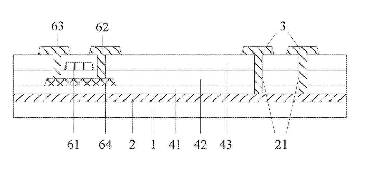
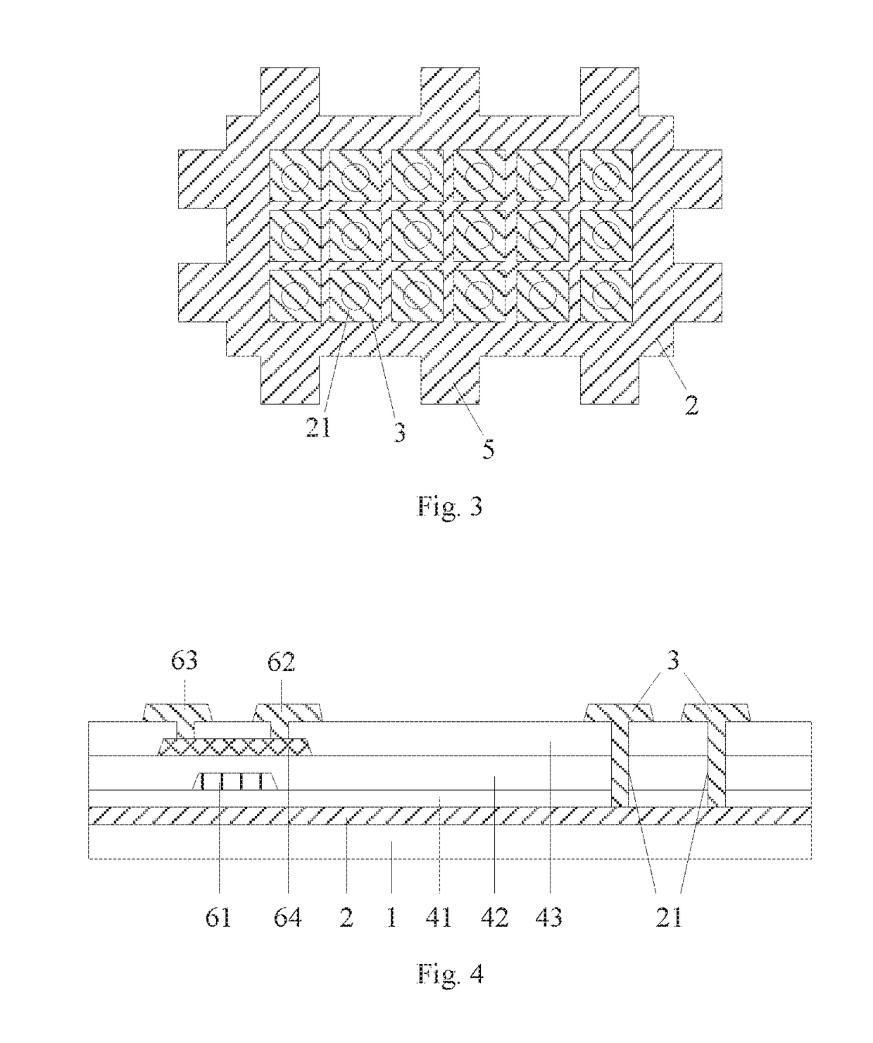
[0028]As shown in FIGS. 3 and 4, an array substrate of an AMOLED display device provided by the present embodiment comprises a baseplate 1, a surface-shaped power line 2, a point-shaped power line 3, and a plurality of insulating layers arranged between the surface-shaped power line 2 and the point-shaped power line 3. According to the present embodiment, the plurality of insulating layers comprise a first insulating layer 41, a second insulating layer 42, and a third insulating layer 43 that are formed from bottom to top in sequence.

[0029]The surface-shaped power line 2 and the point-shaped power line 3 are configured to provide a positive polarity power source to a light-emitting diode. The surface-shaped power line 2 is formed on the baseplate 1, and the point-shaped power line 3 is formed on the plurality of insulating layers. The surface-shaped power line 2 and the point-shaped power line 3 are electrically connected to each other through a via hole 21.

[0030]Further, according ...

embodiment 2

[0035]An array substrate of an AMOLED display device provided by the present embodiment is basically the same as that provided by embodiment 1, and the difference therebetween lies in that: as shown in FIGS. 5 and 6, according to the present embodiment, the metal lead wire 5 and the point-shaped power line 3 are arranged in a same layer, and the metal lead wire 5 and the surface-shaped power line 2 on a baseplate 1 are electrically connected to each other through a via hole.

[0036]Moreover, the array substrate of the present embodiment differs from that of embodiment 1 in that: as shown in FIG. 6, a TFT in the present embodiment has a top gate structure, i.e., a gate is arranged above an active layer.

[0037]Specifically, a gate 61 is formed between a second insulating layer 42 and a third insulating layer 43, and an active layer 64 is formed between a first insulating layer 41 and the second insulating layer 42. A source 62 and a drain 63 are arranged in a same layer as the point-shap...

embodiment 3

[0040]The present embodiment provides an AMOLED display device, which comprises an array substrate provided by embodiment 1 or embodiment 2.

[0041]The AMOLED display device provided by the present embodiment and the array substrate provided by the above embodiments have same technical features, and thus they can solve same technical problem and achieve same technical effect.


PUM


Abstract

An AMOLED display device and an array substrate thereof are disclosed. The array substrate of the AMOLED display device includes a baseplate, a surface-shaped power line, a point-shaped power line, and a plurality of insulating layers arranged between the surface-shaped power line and the point-shaped power line. The surface-shaped power line and the point-shaped power line are configured to provide a positive polarity power source to a light-emitting diode. The surface-shaped power line is formed on the baseplate, and the point-shaped power line is formed on the plurality of insulating layers. The surface-shaped power line and the point-shaped power line are electrically connected to each other through a via hole.

Description

CROSS REFERENCE TO RELATED APPLICATIONS[0001]The present application claims the priority of Chinese patent application CN201610794566.5, entitled “AMOLED display device and array substrate thereof” and filed on Aug. 31, 2016, the entirety of which is incorporated herein by reference.FIELD OF THE INVENTION[0002]The present disclosure relates to the technical field of display, and particularly to an AMOLED display device and an array substrate thereof.BACKGROUND OF THE INVENTION[0003]With the development of display technologies, Active Matrix Organic Light-Emitting Diode (AMOLED) display technology gradually becomes mature and AMOLED display devices are increasingly used in different display fields.[0004]A basic driving unit in an AMOLED display device is shown in FIG. 1. The driving unit comprises two thin-film transistors (TFT) and a storage capacitor Cst to form a 2T1C structure. A scanning signal Vgate is input to a gate of a first thin-film transistor, and a data signal Vdata is ...

Claims


Application Information

Patent Timeline
Patent Type & Authority Applications(United States)
IPC IPC(8): H01L27/32
CPCH01L27/3276H01L27/3262H01L27/3258H10K59/1315H10K59/123H10K59/131H10K59/00H10K59/10H10K59/124H10K59/127H10K59/1213
Inventor HAN, BAIXIANG
Owner SHENZHEN CHINA STAR OPTOELECTRONICS TECH CO LTD
Why Eureka
Try Eureka