Testkey structure and method of measuring device defect or connection defect by using the same

a testkey and structure technology, applied in the direction of electrical testing, measurement devices, instruments, etc., can solve the problems of increasing the difficulty of measuring the resistance value of the finfet, many problems would rise, and the current planar fet no longer meets the requirements of the products, etc., to achieve easy operation, easy design, and rapid scanning of the array

Active Publication Date: 2018-10-11
UNITED MICROELECTRONICS CORP
View PDF3 Cites 0 Cited by
  • Summary
  • Abstract
  • Description
  • Claims
  • Application Information

AI Technical Summary

Benefits of technology

[0008]Since the testkey structure is simply and is easy to operate, it can be easily designed as an array so as to gain lots of sample results by quickly scanning the array. Thus, the time for obtaining the sample result and evaluating device defect or connection defect can be greatly saved.

Problems solved by technology

However, with the increasing miniaturization of electronic products, current planar FETs no longer meet the requirements of the products.
However, many problem would raise because the shrinkage of the FinFETs size.
For example, measuring a resistance value of a FinFET would become more difficult because additional components should be added into original circuits, taking extra space and affecting original design of the products.

Method used


Image

  • Testkey structure and method of measuring device defect or connection defect by using the same
  • Testkey structure and method of measuring device defect or connection defect by using the same
  • Testkey structure and method of measuring device defect or connection defect by using the same

Examples


Embodiment Construction

[0017]To provide a better understanding of the presented invention, preferred embodiments will be described in detail. The preferred embodiments of the present invention are illustrated in the accompanying drawings with numbered elements.

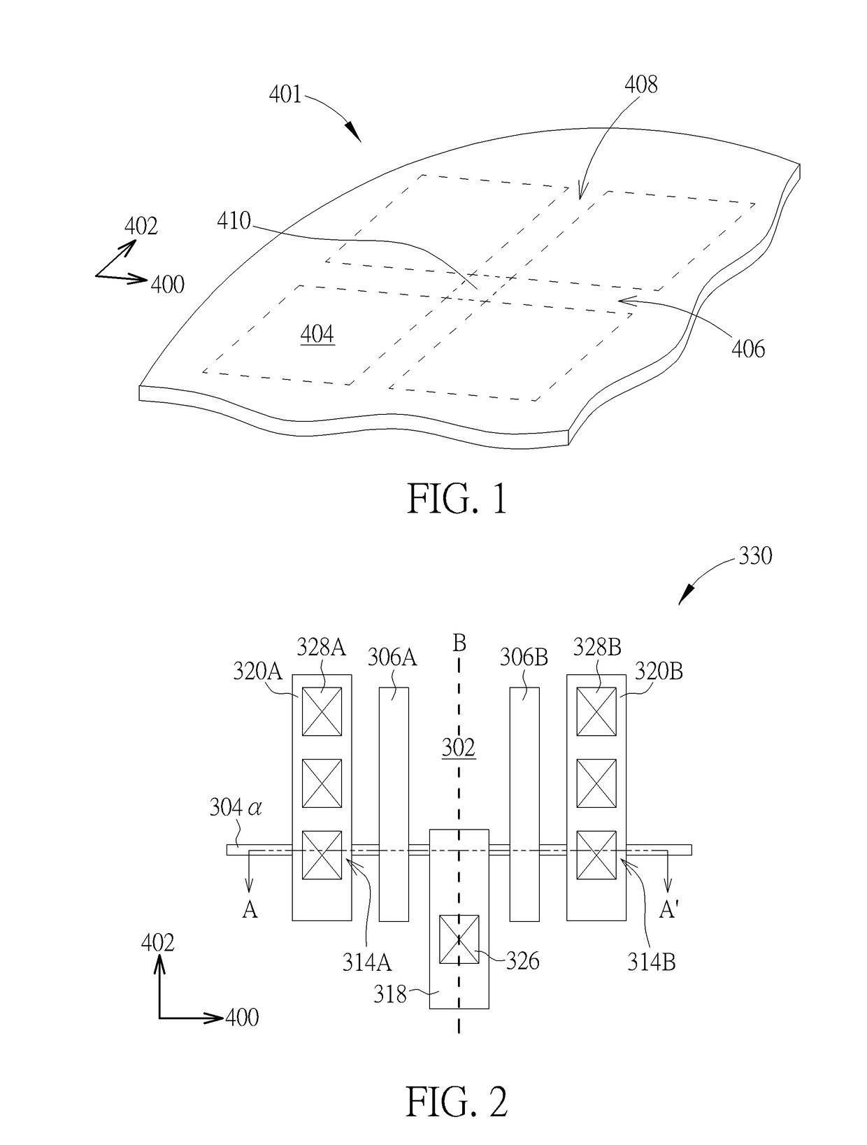
[0018]Please refer to FIG. 1, which show a schematic diagram of the testkey structure on a wafer according to one embodiment of the present invention. As shown in FIG. 1, a wafer 401 including a plurality of die regions 404, a plurality of first scribing line regions 406 stretching along a first direction 400 and a plurality of second scribing line regions 408 stretching along a second direction 402 are provided. In one embodiment, the first direction 400 is perpendicular to the second direction 402. Preferably, the die regions 404 are arranged in an array manner and the die regions 404 are separated from each other by the first scribe line regions 406 and the second scribe line regions 408. In the subsequent process, various semiconductor structure...


PUM


Abstract

A testkey structure including the following components is provided. A fin structure is disposed on a substrate and stretches along a first direction. A first gate structure and a second gate structure are disposed on the fin structure and stretch along a second direction. A first common source region is disposed in the fin structure between the first gate structure and the second gate structure. A first drain region is disposed in the fin structure at a side of the first gate structure opposite to the first common source region. A second drain region disposed in the fin structure at a side of the second gate structure opposite to the first common source region. A testkey structure is symmetrical along a horizontal line crossing the first common source region. The present invention further provides a method of measuring device defect or connection defect by using the same.

Description

BACKGROUND OF THE INVENTION1. Field of the Invention[0001]The present invention relates to a testkey structure and a method of using the same to measure device defect or connection defect.2. Description of the Prior Art[0002]In recent years, as various kinds of consumer electronic products are being constantly modified towards increased miniaturization, the size of semiconductor components are modified to be reduced accordingly, in order to meet high integration, high performance, low power consumption, and the demands of products.[0003]However, with the increasing miniaturization of electronic products, current planar FETs no longer meet the requirements of the products. Thus, non-planar FETs such as Fin-shaped FETs (FinFET) have been developed, which includes a three-dimensional channel structure. The manufacturing processes of FinFET devices can be integrated into traditional logic device processes, and thus are more compatible. In addition, since the three-dimensional structure ...

Claims


Application Information

Patent Timeline
Patent Type & Authority Applications(United States)
IPC IPC(8): G01R31/26
CPCG01R31/2621G01R31/2601G01R31/2644
Inventor WU, KUEI-SHENGLIAO, WEN-JUNGHSIAO, WEN-SHAN
Owner UNITED MICROELECTRONICS CORP
Why Eureka
Try Eureka