Optoelectronic package

a technology of optoelectronic and package, applied in the direction of basic electric elements, electrical apparatus, semiconductor devices, etc., can solve the problem of difficult uniform emission of light rays, and achieve the effect of increasing the viewing angle of the optoelectronic packag

Inactive Publication Date: 2018-10-18
UNISTARS
View PDF4 Cites 1 Cited by
  • Summary
  • Abstract
  • Description
  • Claims
  • Application Information

AI Technical Summary

Benefits of technology

[0015]The optoelectronic package according to the invention employs the optical scattering layer and the optical sealant to diffuse the light rays, so as to increase the viewing angle of the optoelectronic package, thereby emitting the light rays uniformly. Compared with the conventional LED, the optoelectronic package according to the invention is more applicable to the production of making the lamp having a wide range of illumination, such as a ceiling light.

Problems solved by technology

Generally, each of the most LEDs has a small viewing angle, so that the LED emits light rays in a concentrated manner, thereby causing that the LED to be difficult of emitting the light rays uniformly.

Method used


Image

  • Optoelectronic package
  • Optoelectronic package
  • Optoelectronic package

Examples


Embodiment Construction

[0019]The present invention will now be described more specifically with reference to the following embodiments. It is to be noted that the following descriptions of the preferred embodiments of this invention are presented herein for the purpose of illustration and description only. It is not intended to be exhaustive or to be limited to the precise form disclosed.

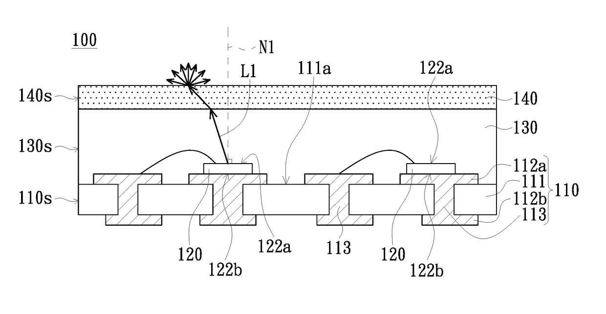
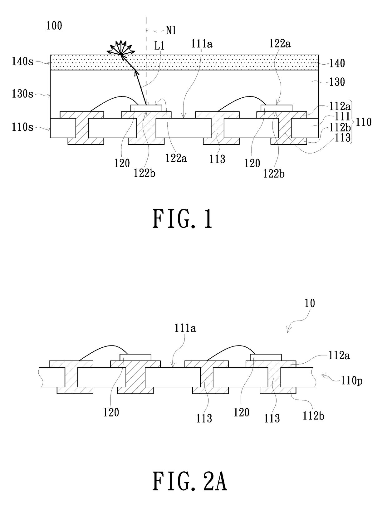
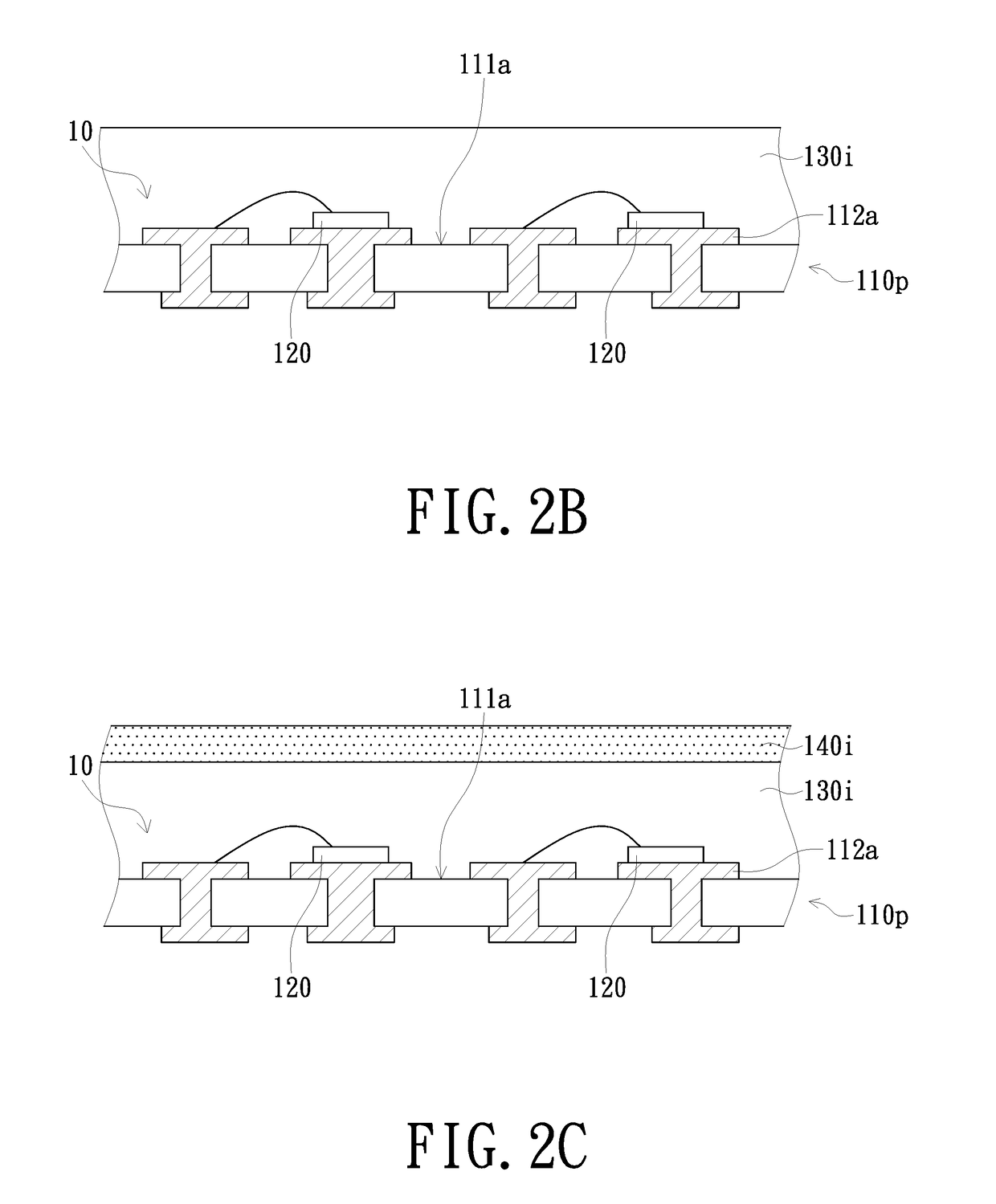
[0020]FIG. 1 is a schematic cross-sectional view of an optoelectronic package according to an embodiment of the present invention. Referring to FIG. 1, an optoelectronic package 100 includes a substrate 110 and at least one light emitting chip 120, in which the light emitting chip 120 is mounted on the substrate 110. The substrate 110 has a carrying plane 111a, whereas the light emitting chip 120 has a light emitting surface 122a and a back surface 122b opposite to the light emitting surface 122a thereof. The back surface 122b of the light emitting chip 120 faces to the carrying plane 111a and a wiring layer 112a of the s...


PUM


Abstract

An optoelectronic package includes a substrate, a light emitting chip, an optical sealant, and an optical scattering layer. The substrate has a carrying plane and a wiring layer formed on the carrying plane. The light emitting chip used for emitting a light ray is mounted on the carrying plane and electrically connected to the wiring layer. The optical sealant covers the carrying plane and wraps the light emitting chip. The optical sealant is located in the path of the light ray. The optical scattering layer covers the optical sealant. The optical sealant located in the path of the light ray is formed between the substrate and the optical scattering layer. Preferably, the refractive index of the optical sealant is larger than or equal to the refractive index of the optical scattering layer.

Description

FIELD OF THE INVENTION[0001]The present invention relates to an optoelectronic package, and more particularly to an optoelectronic package having an optical scattering layer.BACKGROUND OF THE INVENTION[0002]A Light Emitting Diode (LED) is a semiconductor package and has a diode die that is capable of emitting light rays. Generally, each of the most LEDs has a small viewing angle, so that the LED emits light rays in a concentrated manner, thereby causing that the LED to be difficult of emitting the light rays uniformly. Accordingly, the LED is suitable for making a lamp having a narrow range of illumination (or narrow beam angle), such as a flashlight. However, making a lamp used for a wide range of illumination (or wider beam angle), such as a ceiling light (i.e. ceiling fitting), requires of adding additional optical components for producing better or improved illuminating effect.SUMMARY OF THE INVENTION[0003]The present invention provides an optoelectronic package that has an opti...

Claims


Application Information

Patent Timeline
Patent Type & Authority Applications(United States)
IPC IPC(8): H01L51/52H01L51/10
CPCH01L51/5268H01L51/524H01L51/5275H01L51/107H01L33/52H01L33/56H01L33/58H01L33/50H01L33/62H01L2933/0091H10K50/854H10K10/88H10K50/841H10K50/858
Inventor WU, SHANG-YIHSIEH, HSIN-HSIEN
Owner UNISTARS
Why Eureka
Try Eureka