Board mounted LED array

a led array and led array technology, applied in the direction of semiconductor devices for light sources, light and heating apparatus, printed circuit aspects, etc., can solve the problems of e-panels still having a cost penalty due to unused pcb, e-panel design does not allow an initial board, e-panel design is therefore not very versatile, etc., and achieves the effect of maximizing the use of board materials

Inactive Publication Date: 2018-10-25
SIGNIFY HLDG BV
View PDF1 Cites 1 Cited by
  • Summary
  • Abstract
  • Description
  • Claims
  • Application Information

AI Technical Summary

Benefits of technology

[0019]This design also provides a larger carrier board area around each lighting element where heat dissipation is needed, and a thinner carrier board area at the interconnecting parts, so that the use of board material is more efficient.

Problems solved by technology

As the trend of higher efficiency and lower cost progresses, the E-panels will still have a cost penalty due to unused PCB area.
The E-panel design does not for example allow an initial board to be cut into more than two identical parts.
The E-panel design is thus not very versatile.

Method used


Image

  • Board mounted LED array
  • Board mounted LED array
  • Board mounted LED array

Examples


Embodiment Construction

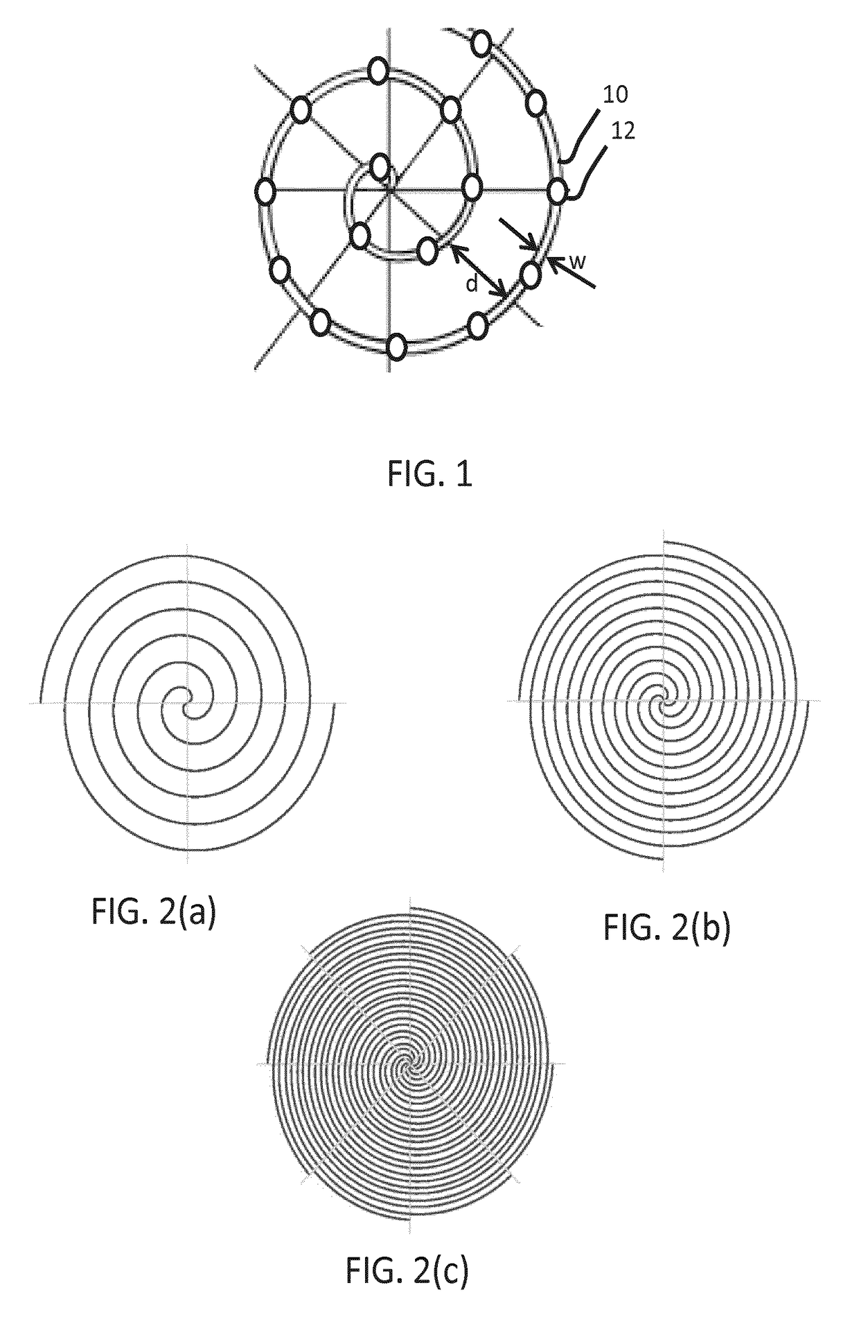
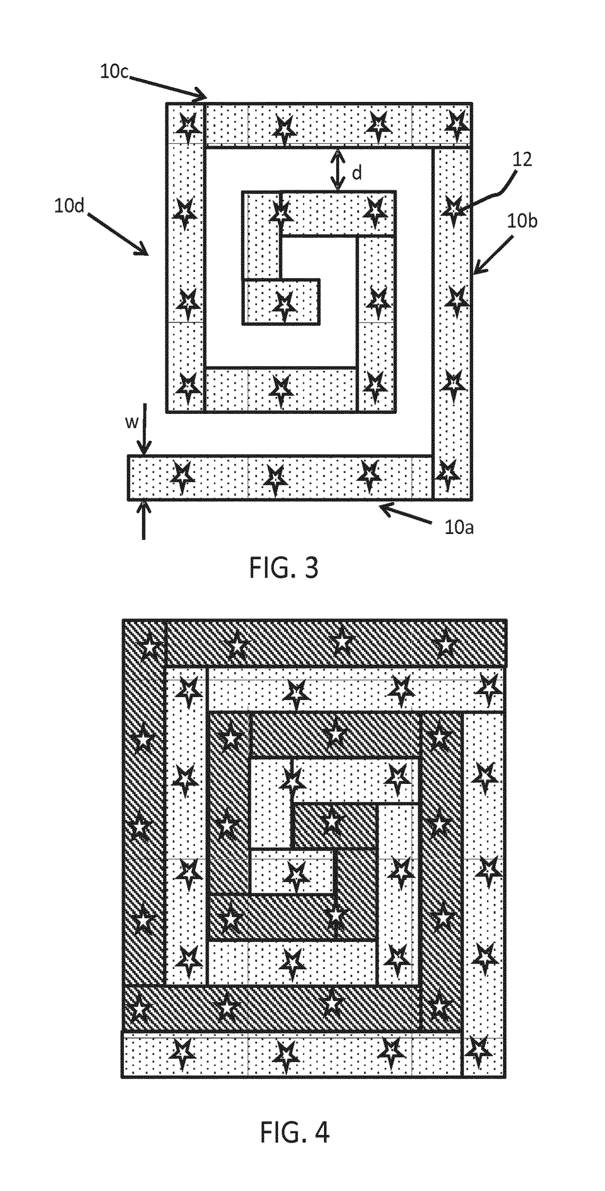
[0038]The invention provides a lighting device comprising a carrier board and an array of lighting elements mounted on the carrier board. The carrier board has a generally spiral or coiled shape and the carrier board can be tessellated with one or more identical other carrier boards with windings interleaved with each other. This enables multiple carrier boards to be formed from a single substrate with little or no waste of material. Different designs enable two, four or even more different identical carrier board shapes to be tessellated together.

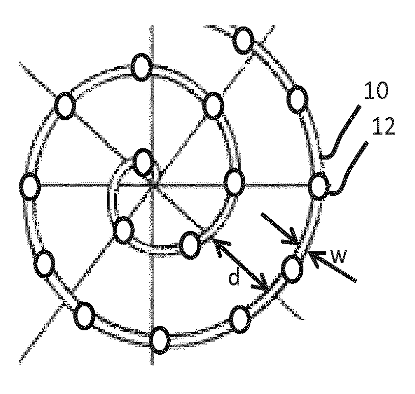
[0039]FIG. 1 shows a first example of lighting device shaped in the form of a spiral. The lighting device comprises a carrier board 10 and an array of lighting elements 12 mounted on the carrier board.

[0040]For all examples in accordance with the invention, the carrier board has a coil shape with multiple converging windings, and the carrier board can be tessellated with one or more identical other carrier boards with the windings interlea...


PUM


Abstract

A lighting device comprising a carrier board and an array of lighting elements mounted on the carrier board. The carrier board has a generally spiral shape and the carrier board can be tessellated with one or more identical other carrier boards with windings interleaved with each other. This enables multiple carrier boards to be formed from a single substrate with little or no waste of material. Different designs enable two, four or even more different identical carried board shapes to be tessellated together.

Description

FIELD OF THE INVENTION[0001]This invention relates to lighting devices and in particular to lighting devices having an array of lighting elements such as LEDs mounted on a board such as a printed circuit board.BACKGROUND OF THE INVENTION[0002]For general illumination, large area light sources are often used in order to provide a low peak brightness and hence to give comfortable low-glare lighting. In LED luminaires having an LED array, the small and bright individual LEDs need to be placed relatively far apart on a large area board, such as a printed circuit board, in order to create a large area light source. Usually such a light source is combined with a diffusive plate or foil to hide the individual LEDs.[0003]The trend of LED technology is for smaller LEDs, increased efficiency (and hence lower thermal dissipation) and lower cost. As a result, the LEDs require less PCB area per LED to meet the required thermal and mechanical design constraints. The PCB cost also becomes a more s...

Claims


Application Information

Patent Timeline
Patent Type & Authority Applications(United States)
IPC IPC(8): F21S4/10F21S4/28F21V29/503F21V29/70
CPCF21S4/10F21S4/28F21V29/503F21V29/70F21Y2115/10H05K2201/09027H05K2201/09127H05K2201/09918H05K2201/10106F21S4/20F21Y2103/10H05K3/0052H05K3/0097H05K2201/09972F21Y2103/20F21Y2103/30
Inventor VISSENBERG, MICHEL CORNELIS JOSEPHUS MARIEWONDERGEM-DE BEST, ANNA WILHELMINA MARIA
Owner SIGNIFY HLDG BV
Why Eureka
Try Eureka