Multilayer electronic component

a technology of electronic components and components, applied in the direction of stacked capacitors, fixed capacitor details, inductances, etc., can solve the problems of increasing the probability of electromagnetic interference between electronic components, and reducing the occurrence of electromagnetic troubles. , to achieve the effect of increasing the packing density

Active Publication Date: 2018-11-01
TDK CORPARATION
View PDF0 Cites 14 Cited by
  • Summary
  • Abstract
  • Description
  • Claims
  • Application Information

AI Technical Summary

Benefits of technology

[0009]It is an object of the present invention to provide a multilayer electronic component configured to prevent the occurrence of electromagnetic troubles associated with increased packing density.
[0018]According to the multilayer electronic components of the first to fifth aspects of the present invention, the shields entirely cover the top surface and the four side surfaces of the multilayer stack, and have the respective additional features. This enables prevention of the occurrence of the electromagnetic troubles associated with increased packing density.

Problems solved by technology

Due to the recent increases in packing density of electronic components, the occurrence of electromagnetic troubles as described below has become an issue of concern.
Specifically, as the spacing between the electronic components is reduced, electromagnetic interference is more likely to occur between the electronic components.
It is thus difficult with the disclosed electronic component to sufficiently reduce the occurrence of the electromagnetic troubles associated with the increased packing density as described above.
However, it is difficult with the shield electrode of a cylindrical shape to sufficiently reduce the occurrence of the electromagnetic troubles.
Even with this example, however, the occurrence of the electromagnetic troubles are not always preventable.

Method used


Image

  • Multilayer electronic component
  • Multilayer electronic component
  • Multilayer electronic component

Examples


first embodiment

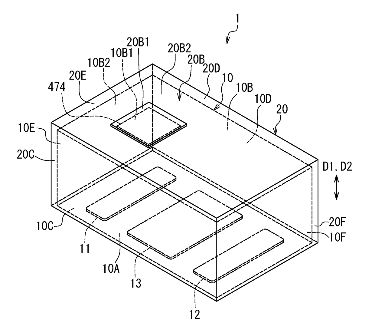
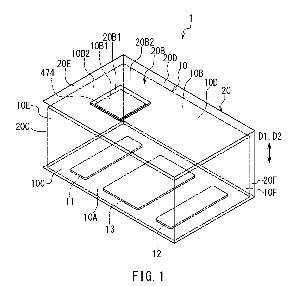
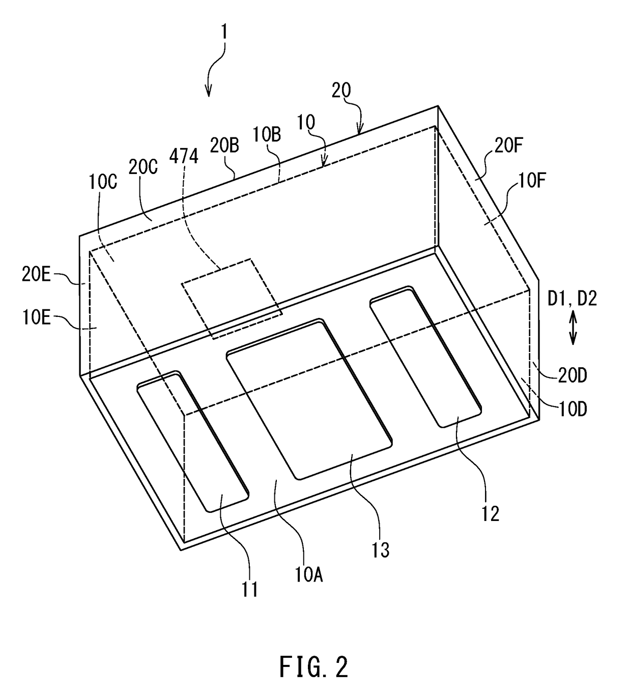
[0050]Preferred embodiments of the present invention will now be described in detail with reference to the drawings. First, reference is made to FIG. 1 to FIG. 4 to describe an example structure of a multilayer electronic component (hereinafter simply referred to as electronic component) 1 according to a first embodiment of the invention. FIG. 1 is an external perspective view of the electronic component 1. FIG. 2 is a perspective view illustrating the bottom of the electronic component 1. FIG. 3 is an internal perspective view of a multilayer stack in the electronic component 1. FIG. 4 is a cross-sectional view of the electronic component 1.

[0051]The electronic component 1 is for use in compact mobile communication apparatuses such as cellular phones and smartphones. The electronic component 1 may have the function of a filter, a balun, a directional coupler or a branching filter, for example.

[0052]The electronic component 1 includes a multilayer stack 10, a plurality of terminals ...

second embodiment

[0134]An electronic component 1 according to a second embodiment of the invention will now be described with reference to FIG. 19 and FIG. 20. FIG. 19 is a perspective view illustrating the bottom of the electronic component 1 according to the second embodiment. FIG. 20 is an explanatory diagram illustrating the patterned surface of the first dielectric layer 31 of the multilayer stack 10 in the second embodiment.

[0135]In the present embodiment, as shown in FIG. 19, the shield 20 includes a bottom covering portion 20A in addition to the top covering portion 20B and the side covering portions 20C to 20F. The bottom covering portion 20A partially covers the bottom surface 10A of the multilayer stack 10 and is connected to the ground terminal without coming into contact with the plurality of signal terminals 11 and 12.

[0136]In the present embodiment, as shown in FIG. 20, conductor layers 311, 312 and 315 are formed on the patterned surface of the first dielectric layer 31 of the multil...


PUM

PropertyMeasurementUnit
thickaaaaaaaaaa
thickaaaaaaaaaa
thickaaaaaaaaaa

Abstract

A multilayer electronic component includes: a multilayer stack including a plurality of dielectric layers and a plurality of conductor layers stacked together; a plurality of terminals integrated with the multilayer stack; and a shield formed of a conductor and integrated with the multilayer stack. The multilayer stack has a top surface, a bottom surface, and four side surfaces connecting the top surface and the bottom surface. The plurality of terminals are provided on the bottom surface of the multilayer stack. The shield entirely covers the top surface and the four side surfaces of the multilayer stack. The shield includes a portion that is thicker than the other portions of the shield.

Description

BACKGROUND OF THE INVENTION1. Field of the Invention[0001]The present invention relates to a multilayer electronic component including a multilayer stack that includes a plurality of dielectric layers and a plurality of conductor layers stacked together.2. Description of the Related Art[0002]Recently, compact mobile communication apparatuses typified by cellular phones and smartphones have achieved greater functionality and further miniaturization, and the packing densities of electronic components have increased accordingly. As a result, spacings between the electronic components mounted on a mount substrate or distances from the electronic components to a shield case covering the electronic components have been reduced in the compact mobile communication apparatuses.[0003]Among known electronic components suitable for miniaturization are multilayer electronic components that are each formed using a multilayer stack including a plurality of dielectric layers and a plurality of cond...

Claims


Application Information

Patent Timeline
Patent Type & Authority Applications(United States)
IPC IPC(8): H01F27/36H01F27/40H01F27/28H01G4/30H01G4/228
CPCH01F27/36H01F27/40H01F27/28H01G4/30H01G4/228H05K9/0007H01F27/363H01F17/0013H01F27/292H03H1/00H01F2017/008H01G4/38H01G4/40H01G4/232
Inventor KUSUMOTO, SHOHEIOOTSUKA, NORIAKIABE, MINORUSATO, YOSHINORI
Owner TDK CORPARATION
Why Eureka
Try Eureka