Solid-state imaging device and electronic device

a solid-state imaging and electronic device technology, applied in the direction of transistors, television systems, radio control devices, etc., can solve the problems of uneven sensitivity (output) of multiple pixels that share fd regions, the layout of pixel transistors and other components is subject to constraints, etc., to suppress the deterioration of pixel characteristics and ensure the operating range of vsls

Active Publication Date: 2018-11-08
SONY CORP
View PDF1 Cites 1 Cited by
  • Summary
  • Abstract
  • Description
  • Claims
  • Application Information

AI Technical Summary

Benefits of technology

[0029]According to the first and the second aspects of the present disclosure, the deterioration of pixel characteristics is suppressed and the operating range of VSLs is guaranteed.

Problems solved by technology

However, the layout of pixel transistors and other components is subject to constraints where the pixel size is refined to approximately 1 μm, for example, even if the above-mentioned pixel sharing technology is used.
In that case, the characteristics such as sensitivity (output) of multiple pixels that share FD regions can become uneven.

Method used


Image

  • Solid-state imaging device and electronic device
  • Solid-state imaging device and electronic device
  • Solid-state imaging device and electronic device

Examples


Embodiment Construction

[0045]The best modes for carrying out the present disclosure (called the embodiments hereunder) are described below in detail with reference to the accompanying drawings.

[0046](First Configuration Example of Pixel Sharing Unit to Which Present Disclosure is Applied)

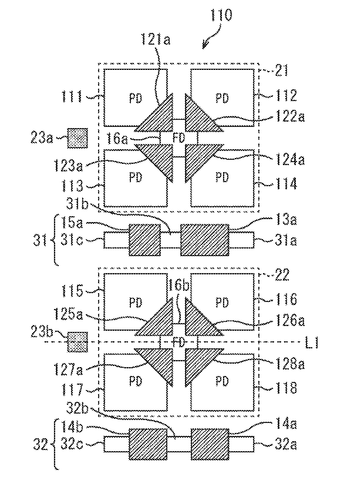
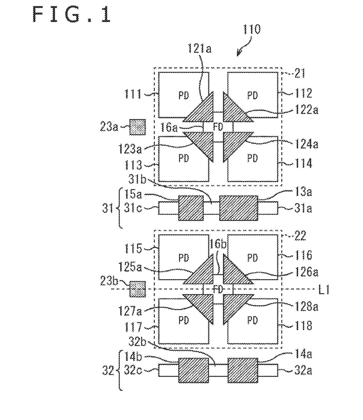
[0047]FIG. 4 illustrates a first configuration example of a pixel sharing unit in a back-illuminated CMOS image sensor as one embodiment of the present disclosure.

[0048]The first configuration example, as with the pixel sharing unit 110 in FIG. 1, has two FD regions shared by eight pixels (PDs). In the first configuration example, the components substantially the same as those in the pixel sharing unit 110 of FIG. 1 are designated by the same reference symbols. Subfigure A in FIG. 4 illustrates a silicon (Si) substrate having a first light receiving section 21 and a second light receiving section 22 formed therein, as well as an inter-wiring layer film having a first transistor group 31 and a second transistor group 32 fo...


PUM


Abstract

The present disclosure relates to a solid-state imaging device and an electronic device for suppressing deterioration of pixel characteristics while guaranteeing the operating range of VSLs. A solid-state imaging device according to a first aspect of this disclosure has multiple pixel sharing units each including multiple photoelectric conversion sections each configured to correspond to a pixel, an accumulation section configured to be shared by the plurality of photoelectric conversion sections and to accumulate charges generated thereby, and multiple transistors configured to control reading of the charges accumulated in the accumulation section. The plurality of transistors in each pixel sharing unit are arranged symmetrically. The plurality of transistors include a transistor that functions as a switch to change conversion efficiency. The present disclosure may be applied to back-illuminated CMOS image sensors, for example.

Description

TECHNICAL FIELD[0001]The present disclosure relates to a solid-state imaging device and an electronic device. More particularly, the disclosure relates ,to a solid-state imaging device and an electronic device adapted to refine the pixel size and lower drive power.BACKGROUND ART[0002]In solid-state imaging devices typified by complementary metal oxide semiconductor (CMOS) image sensors, the increasing number of pixels has been accompanied by a marked tendency to refine the pixel size. In the case of back-illuminated CMOS image sensors, in particular, various layouts for pixel sharing have been proposed by taking advantage of a high degree of freedom in layout design. The sharing involves, for example, allowing multiple pixels (i.e., their corresponding photodiodes (PDs)) to share a floating diffusion (FD) region and various pixel transistors.[0003]However, the layout of pixel transistors and other components is subject to constraints where the pixel size is refined to approximately ...

Claims


Application Information

Patent Timeline
Patent Type & Authority Applications(United States)
IPC IPC(8): H04N5/359H01L27/146H04N5/374H04N5/355H04N5/3745
CPCH04N5/3595H01L27/14645H01L27/14609H01L27/146H04N5/374H04N5/355H04N5/3745H04N25/59H04N25/778H01L27/14612H01L27/14603H01L27/14643H01L27/14636H04N25/625H04N25/57H04N25/76H04N25/77
Inventor SANO, TAKUYAWAKANO, TOSHIFUMI
Owner SONY CORP
Why Eureka
Try Eureka