Semiconductor device and method for manufacturing the same

a technology of semiconductor devices and manufacturing methods, applied in semiconductor devices, semiconductor/solid-state device details, electrical apparatus, etc., can solve the problems of increased manufacturing cost, increased complicated process, so as to reduce the number of mask and manufacturing steps, easy to manufacture, and favorable characteristics

Inactive Publication Date: 2008-10-02
SEMICON ENERGY LAB CO LTD
View PDF41 Cites 22 Cited by
  • Summary
  • Abstract
  • Description
  • Claims
  • Application Information

AI Technical Summary

Benefits of technology

[0019]In the present invention, since a contact hole having a step portion at the side surface can be formed by one etching process, the number of masks and manufacturing steps can be reduced. Therefore, a semiconductor device with favorable characteristics in which variation in thickness or disconnection of a source electrode or a drain electrode formed in the contact hole is prevented can be easily manufactured.
[0020]Further, in the present invention, when the source electrode or the drain electrode is made in contact with a source region or a drain region at the side surface of the contact hole which is formed in the source region or the drain region, since it is not necessary to stop etching at the surface of a semiconductor layer, the etching in formation of the contact hole can be easily controlled. Thus, a semiconductor device in which deterioration of characteristics is suppressed can be easily manufactured.

Problems solved by technology

However, in Reference 2, the contact hole having the step portion at the side surface of the insulating layer is formed by etching the insulating layer by two etching processes; thus, there have been problems in that the number of masks and manufacturing steps are increased, the process becomes complicated, and the manufacturing cost is increased.
In addition, even when the method for forming a wiring described in Reference 2 is used, the problems of the conventional thin film transistors are kept unsolved.
Therefore, it has been difficult to control etching in formation of the opening in the insulating layer.
This is particularly serious when the semiconductor layer is formed of a thin film with a thickness of 50 nm or less.

Method used


Image

  • Semiconductor device and method for manufacturing the same
  • Semiconductor device and method for manufacturing the same
  • Semiconductor device and method for manufacturing the same

Examples


embodiment mode 1

[0039]In this embodiment mode, a structure of a semiconductor device in which variation in thickness or disconnection of a source electrode or a drain electrode is prevented and a method for manufacturing the semiconductor device will be described,

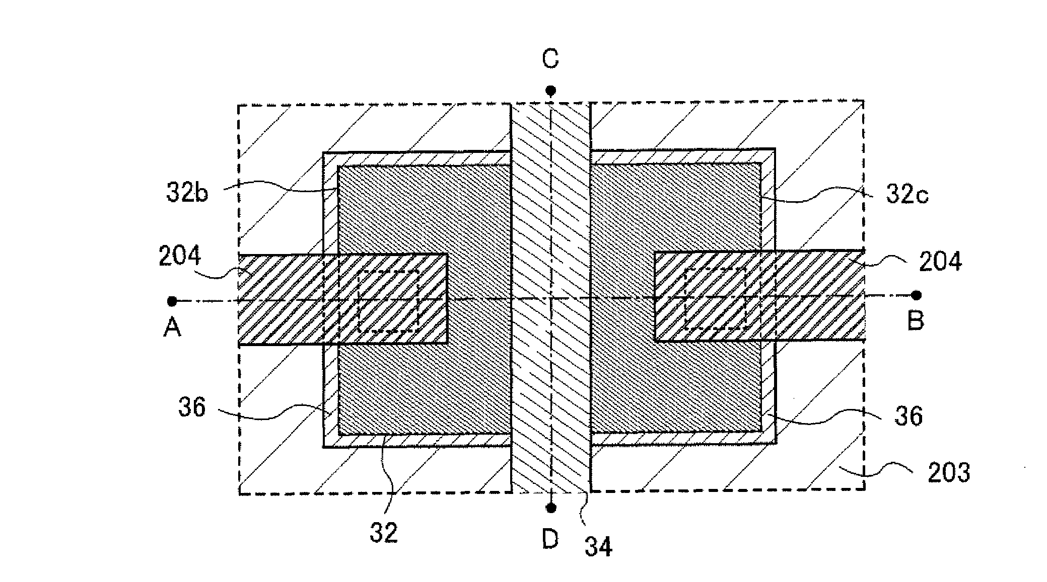
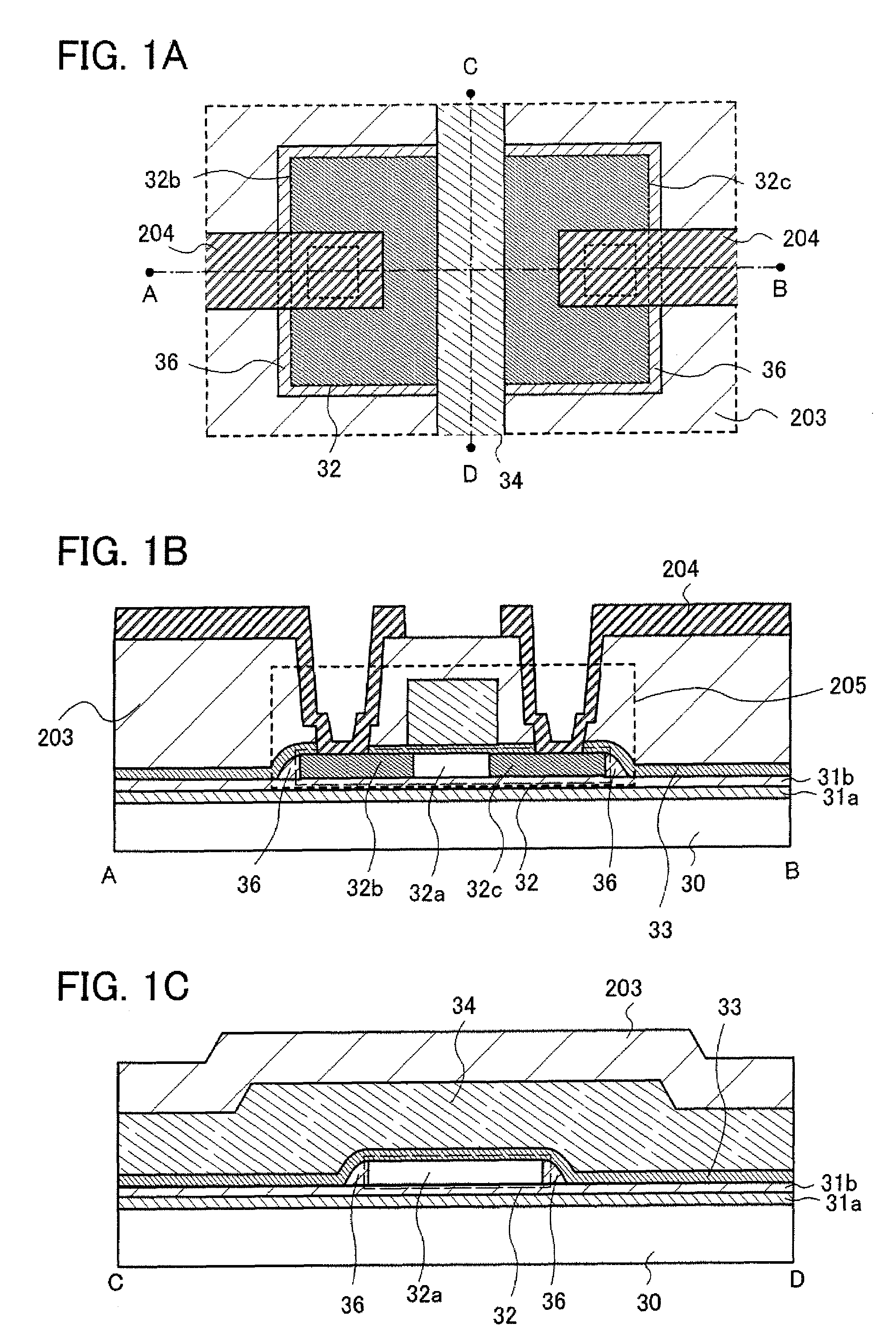
[0040]FIG. 1A is a top view and FIGS. 1B and 1C are cross-sectional views for explaining a main structure of a semiconductor device of the present invention. FIG. 1A is a top view which shows a thin film transistor. FIG. 1B shows a cross section taken along a broken line joining A and B in FIG. 1A. FIG. 1C shows a cross section taken along a broken line joining C and D in FIG. 1A.

[0041]A semiconductor device described in this embodiment mode includes a thin film transistor 205 having an island-shaped semiconductor layer 32 which is provided over a substrate 30 with an insulating layer 31 interposed therebetween, a gate insulating layer 33 formed over the semiconductor layer 32, and a conductive layer 34 which serves as a gate electrode and...

embodiment mode 2

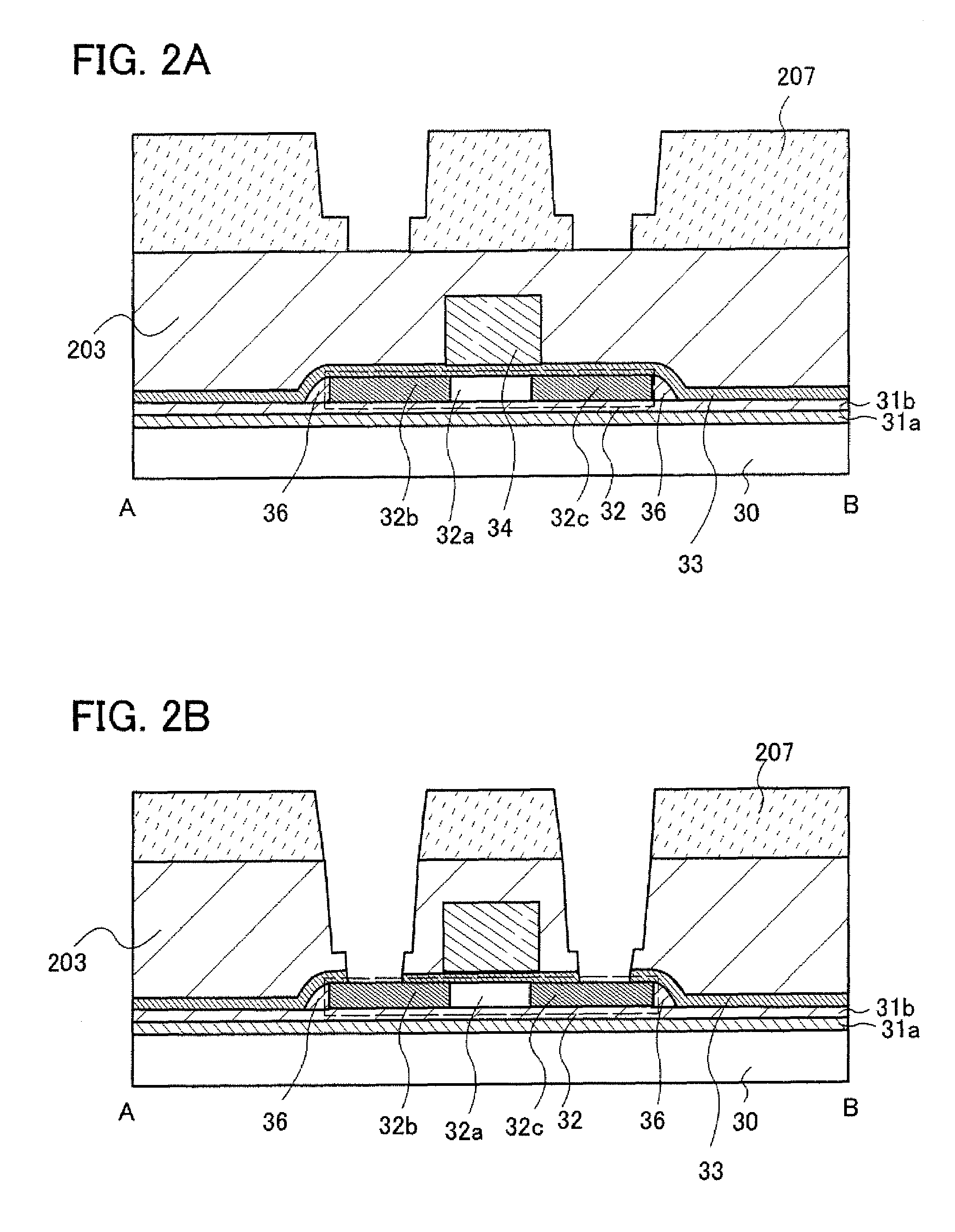
[0064]In this embodiment mode, manufacturing steps of the semiconductor device shown in FIGS. 1A to 1C or FIG. 5 will be specifically described. In this embodiment mode, manufacturing steps which relate to the cross section taken along the broken line joining A and B in FIG. 1A are described with reference to FIGS. 6A to 6D and 7A to 7C, and manufacturing steps which relate to the cross section taken along the broken line joining C and D in FIG. 1A are described with reference to FIGS. 6E to 6H and 7D to 7F.

[0065]First, the insulating layer 31 is formed over the substrate 30 (FIGS. 6A and 6E). In this embodiment mode, the insulating layer 31 has a two-layer structure of the first insulating layer 31a formed over the substrate 30 and the second insulating layer 31b formed over the first insulating layer 31a.

[0066]As the substrate 30, a glass substrate, a quartz substrate, a metal substrate (for example, a ceramic substrate or a stainless steel substrate), a semiconductor substrate s...

embodiment mode 3

[0099]The semiconductor device according to the present invention can have various structures, not limited to those in Embodiment Modes 1 and 2. In this embodiment mode, a structure of a thin film transistor in which a semiconductor layer is partially made silicide and a method for manufacturing the thin film transistor will be described. FIGS. 5A to 5C show a structure of a semiconductor device of this embodiment mode. FIG. 5A is a top view, FIG. 8B shows a cross section taken along a broken line A-B in FIG. 8A, and FIG. 8C shows a cross section taken along a broken line C-D in FIG. 8A.

[0100]As shown in FIGS. 8A to 8C, in the semiconductor device of this embodiment mode, a silicide region 1102 is formed in part of the surface of a semiconductor layer 32 in addition to the structure shown in FIGS. 1A to 1C. In addition, a conductive layer 34 which serves as a gate electrode is formed of a stacked-layer structure of a first conductive layer 34a and a second conductive layer 34b. At t...


PUM


Abstract

A method for easily manufacturing a semiconductor device in which variation in thickness or disconnection of a source electrode or a drain electrode is prevented is proposed A semiconductor device includes a semiconductor layer formed over an insulating substrate; a first insulating layer formed over the semiconductor layer; a gate electrode formed over the first insulating layer; a second insulating layer formed over the gate electrode; an opening which reaches the semiconductor layer and is formed at least in the first insulating layer and the second insulating layer; and a step portion formed at a side surface of the second insulating layer in the opening.

Description

BACKGROUND OF THE INVENTION[0001]1. Field of the Invention[0002]The present invention relates to a semiconductor device and a manufacturing method thereof. In this specification, the semiconductor device refers to any device which can function with the use of semiconductor characteristics.[0003]2. Description of the Related Art[0004]In recent years, there has been extensive production of semiconductor devices in which a thin film transistor (a TFT) is formed over a substrate such as a glass substrate which has an insulating surface and used as a switching element or the like. In the thin film transistor, an island-shaped semiconductor layer is formed over a substrate having an insulating surface by a CVD method, a photolithography process, or the like, and part of the island-shaped semiconductor layer is used as a channel formation region of the transistor (for example, see Reference 1: Japanese Published Patent Application No. H08-018055).[0005]An example of a schematic cross-secti...

Claims


Application Information

Patent Timeline
Patent Type & Authority Applications(United States)
IPC IPC(8): H01L23/52H01L21/28
CPCH01L21/76804H01L23/485H01L29/41733H01L27/124H01L2924/0002H01L2924/00H01L29/78618H01L29/78639H01L29/78606H01L27/12H01L27/1214H01L29/78636
Inventor SASAGAWA, SHINYA
Owner SEMICON ENERGY LAB CO LTD
Why Eureka
Try Eureka