Semiconductor device and method for manufacturing the same

a technology of semiconductor devices and semiconductor layers, which is applied in the direction of semiconductor devices, semiconductor/solid-state device details, electrical apparatus, etc., can solve the problems of difficult control of etching in the formation of the opening in the insulating layer, and achieve the effect of easy manufacturing, suppressing deterioration of characteristics, and easy control

Active Publication Date: 2010-07-27
SEMICON ENERGY LAB CO LTD
View PDF47 Cites 12 Cited by
  • Summary
  • Abstract
  • Description
  • Claims
  • Application Information

AI Technical Summary

Benefits of technology

[0007]The present invention discloses a technique to solve such a problem and provides a technique of manufacturing a semiconductor device in which etching in formation of a contact hole can be easily controlled.
[0013]In the present invention, since it is not necessary to stop etching at the surface of a semiconductor layer, etching in formation of a contact hole can be easily controlled. Further, a source electrode or a drain electrode can be electrically connected to the semiconductor layer at the side surface of the contact hole which is formed in the semiconductor layer; thus, a semiconductor device in which deterioration of characteristics is suppressed can be easily manufactured.

Problems solved by technology

Therefore, it has been difficult to control etching in formation of the opening in the insulating layer.
This is particularly serious when the semiconductor layer is formed of a thin film with a thickness of 50 nm or less.

Method used


Image

  • Semiconductor device and method for manufacturing the same
  • Semiconductor device and method for manufacturing the same
  • Semiconductor device and method for manufacturing the same

Examples


embodiment mode 1

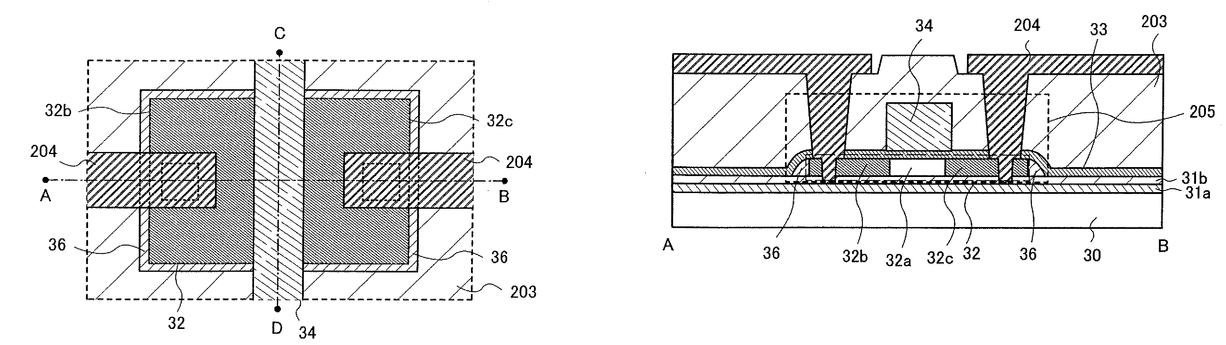
[0036]In this embodiment mode, a structure of a semiconductor device in which etching in formation of a contact hole can be easily controlled and a method for manufacturing the semiconductor device will be described.

[0037]FIG. 1A is a top view and FIGS. 1B and 1C are cross-sectional views for explaining a main structure of a semiconductor device of the present invention. FIG. 1A is a top view which shows a thin film transistor. FIG. 1B shows a cross section taken along a broken line joining A and B in FIG. 1A. FIG. 1C shows a cross section taken along a broken line joining C and D in FIG. 1A.

[0038]A semiconductor device described in this embodiment mode includes a thin film transistor 205 having an island-shaped semiconductor layer 32 which is provided over a substrate 30 with an insulating layer 31 interposed therebetween, a gate insulating layer 33 formed over the semiconductor layer 32, and a conductive layer 34 which serves as a gate electrode and is provided over the semiconduc...

embodiment mode 2

[0078]In this embodiment mode, a structure of a semiconductor device which is different from that in FIGS. 1A to 1C and a method for manufacturing the semiconductor device will be described.

[0079]FIG. 5A is a top view and FIGS. 5B and 5C are cross-sectional views for explaining a structure of a semiconductor device of this embodiment mode. FIG. 5A is a top view which shows a thin film transistor. FIG. 5B shows a cross section taken along a broken line joining A and B in FIG. 5A. FIG. 5C shows a cross section taken along a broken line joining C and D in FIG. 5A.

[0080]A semiconductor device described in this embodiment mode includes a thin film transistor 205 having an island-shaped semiconductor layer 32 which is provided over a substrate 30 with an insulating layer 31 interposed therebetween, a gate insulating layer 33 formed over the semiconductor layer 32, and a conductive layer 34 which serves as a gate electrode and is provided over the semiconductor layer 32 with the gate insul...

embodiment mode 3

[0088]In this embodiment mode, a structure of a semiconductor device which is different from those in FIGS. 1A to 1C and 5A to 5C and a method for manufacturing the semiconductor device will be described.

[0089]FIG. 7A is a top view and FIGS. 7B and 7C are cross-sectional views for explaining a structure of a semiconductor device of this embodiment mode. FIG. 7A is a top view which shows a thin film transistor. FIG. 7B shows a cross section taken along a broken line joining A and B in FIG. 7A. FIG. 7C shows a cross section taken along a broken line joining C and D in FIG. 7A.

[0090]As shown in FIGS. 7A to 7C, in the semiconductor device of this embodiment mode, the shape of a contact hole in which a conductive layer 204 is filled is different from that in the structure shown in FIGS. 5A to 5C. That is, in the semiconductor device described in this embodiment mode, contact holes which reach an insulating layer 31a and are formed by etching an insulating layer 203, impurity regions 32b ...


PUM


Abstract

A technique of manufacturing a semiconductor device in which etching in formation of a contact hole can be easily controlled is proposed. A semiconductor device includes at least a semiconductor layer formed over an insulating surface; a first insulating layer formed over the semiconductor layer; a gate electrode formed over the first insulating layer; a second insulating layer formed over the gate electrode; and a conductive layer formed over the second insulating layer connected to the semiconductor layer via an opening which is formed at least in the semiconductor layer and the second insulating layer and partially exposes the insulating surface. The conductive layer is electrically connected to the semiconductor layer at the side surface of the opening which is formed in the semiconductor layer.

Description

BACKGROUND OF THE INVENTION[0001]1. Field of the Invention[0002]The present invention relates to a semiconductor device and a manufacturing method thereof. In this specification, the semiconductor device refers to any device which can function with the use of semiconductor characteristics.[0003]2. Description of the Related Art[0004]In recent years, there has been extensive production of semiconductor devices in which a thin film transistor (a TFT) is formed over a substrate such as a glass substrate which has an insulating surface and used as a switching element or the like. In the thin film transistor, an island-shaped semiconductor layer is formed over a substrate having an insulating surface by a CVD method, a photolithography process, or the like, and part of the island-shaped semiconductor layer is used as a channel formation region of the transistor (for example, see Reference 1: Japanese Published Patent Application No. H08-018055).[0005]A schematic cross-sectional view of a...

Claims


Application Information

Patent Timeline
Patent Type & Authority Patents(United States)
IPC IPC(8): H01L23/52
CPCH01L21/76802H01L29/41733H01L27/124H01L23/485H01L2924/0002H01L2924/00H01L21/76804H01L21/76805H01L29/78606H01L29/78636H10K59/123H10K59/124
Inventor YAMAZAKI, SHUNPEISUZAWA, HIDEOMISASAGAWA, SHINYAKURATA, MOTOMU
Owner SEMICON ENERGY LAB CO LTD
Why Eureka
Try Eureka