
Liquid crystal display panel and method for manufacturing same

a technology of liquid crystal display panel and liquid crystal molecules, which is applied in the direction of optics, semiconductor devices, instruments, etc., can solve the problems of uniform intensity distribution of light used in the exposure step for forming photo spacers, and achieve the effect of suppressing the drop in display quality caused by disordered alignment of liquid crystal molecules near photo spacers

Active Publication Date: 2019-01-31
SHARP KK
View PDF10 Cites 8 Cited by
  • Summary
  • Abstract
  • Description
  • Claims
  • Application Information

AI Technical Summary

Benefits of technology

The present invention helps to improve the quality of liquid crystal displays by preventing a decrease in the alignment of liquid crystal molecules near photo spacers without reducing the aperture ratio.

Problems solved by technology

This is because an active matrix substrate has, for example, TFTs, gate bus lines, source bus lines, and the like on the surface of a glass substrate, and thus the surface is not necessarily flat; furthermore, the intensity distribution of light used in the exposure step for forming the photo spacers is not uniform.

Method used


Image

  • Liquid crystal display panel and method for manufacturing same
  • Liquid crystal display panel and method for manufacturing same
  • Liquid crystal display panel and method for manufacturing same

Examples


first embodiment

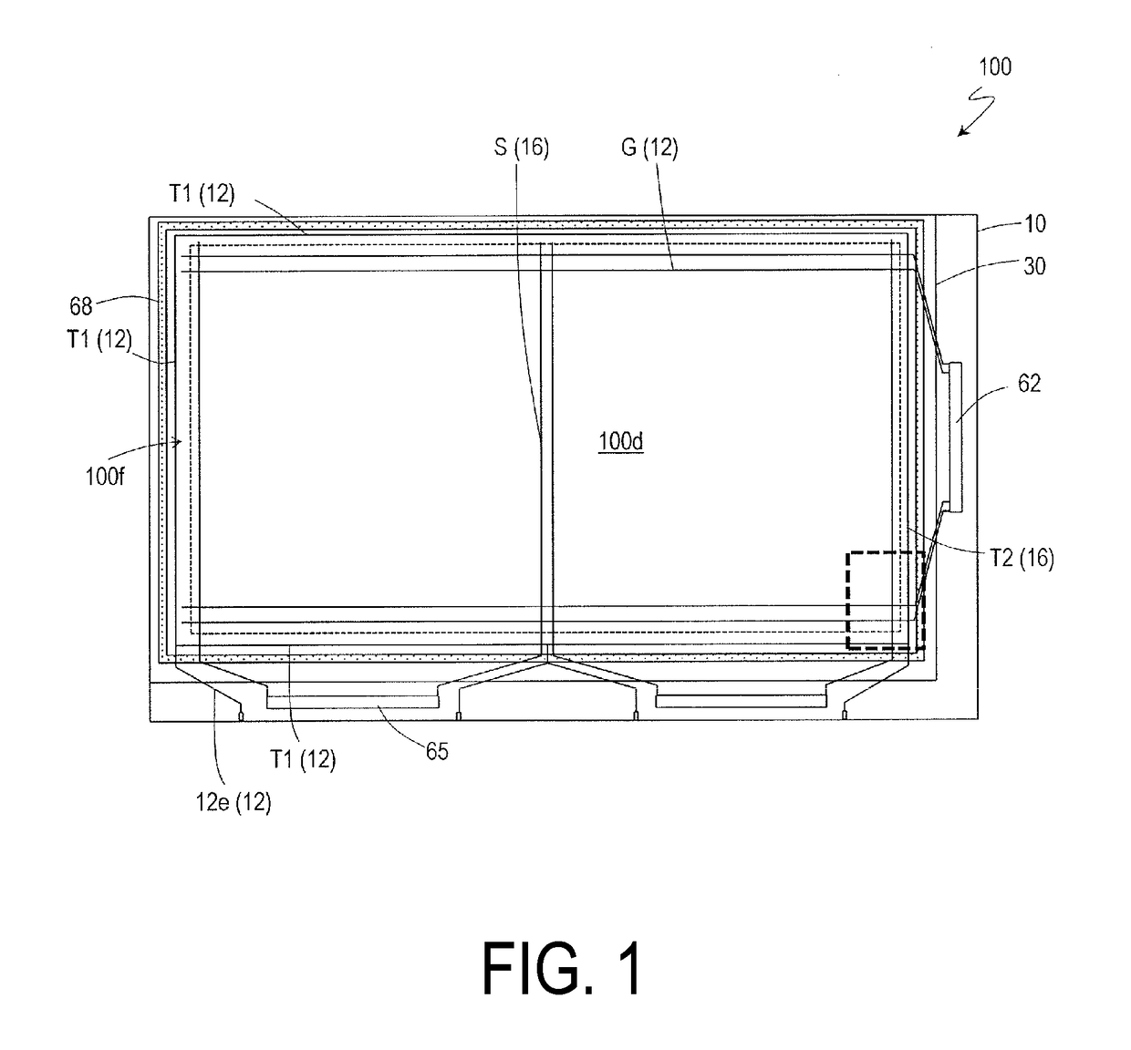
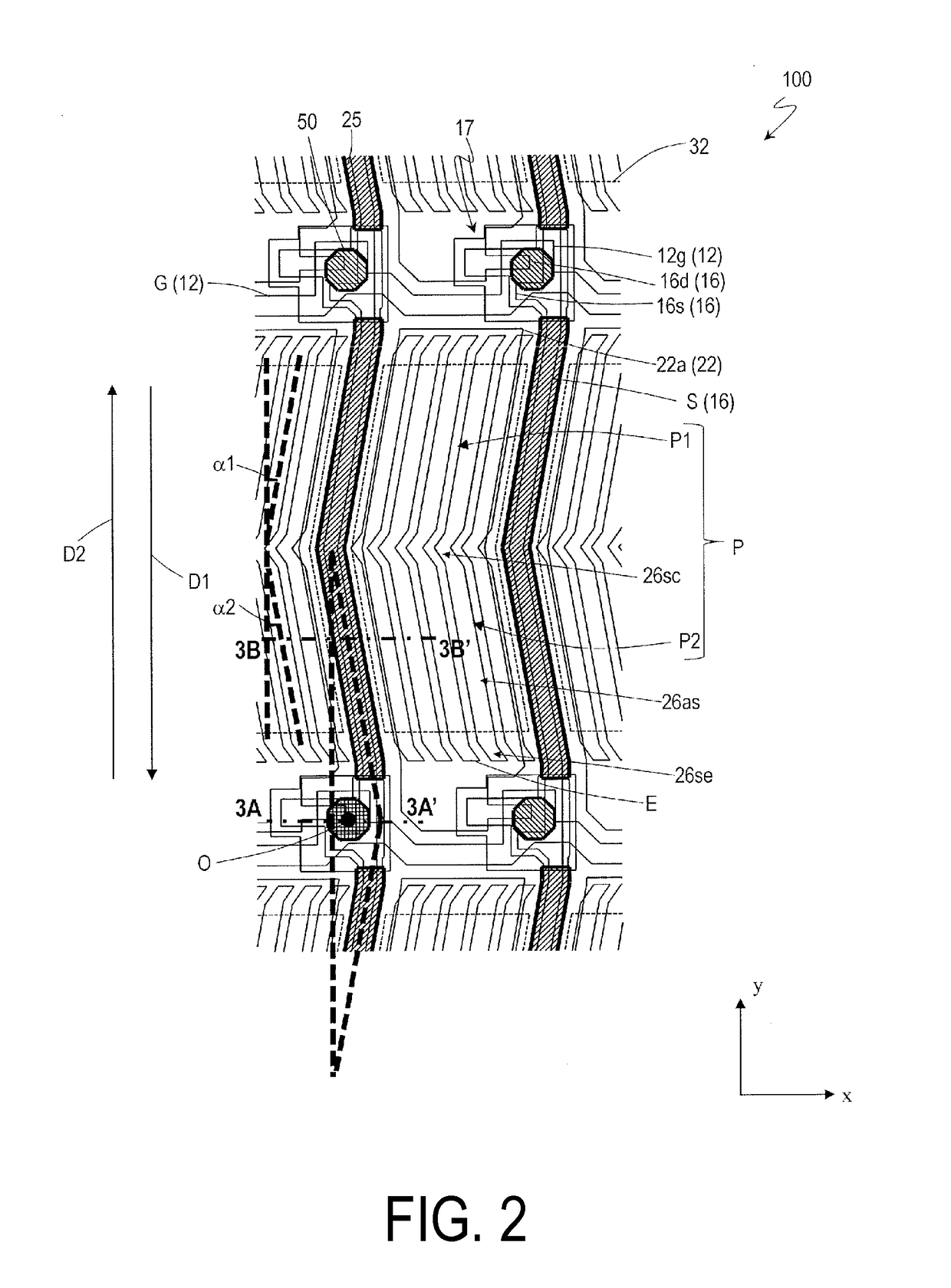
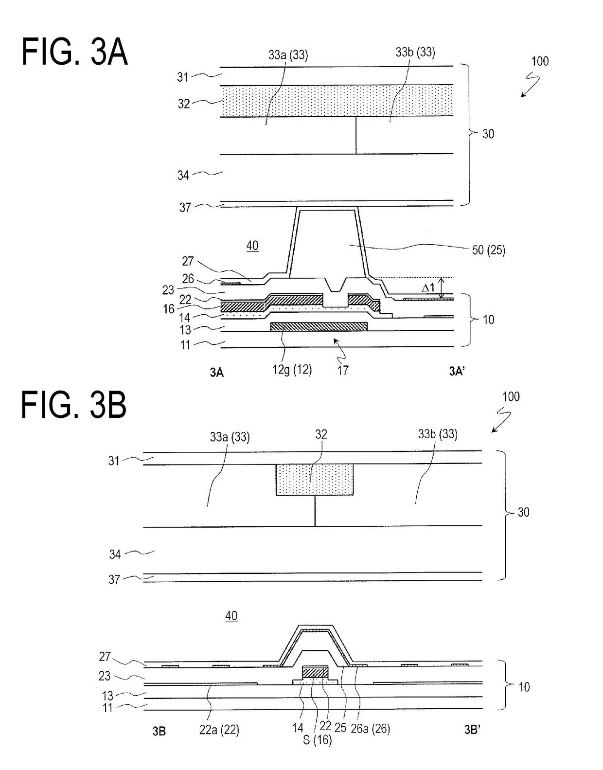
[0077]A liquid crystal display panel 100 according to a first embodiment of the present invention will be described with reference to FIGS. 1 to 3B. FIG. 1 is a plan view schematically illustrating the liquid crystal display panel 100. FIGS. 2 to 3B are a plan view and cross-sectional views schematically illustrating the structure of a display region in the liquid crystal display panel 100. FIGS. 3A and 3B are diagrams illustrating the cross-sectional structure of the display region in the liquid crystal display panel 100, respectively taken along a line 3A-3A′ and a line 3B-3B′ in FIG. 2.

[0078]Although the liquid crystal display panel 100 illustrated here is a FFS mode liquid crystal display panel, the liquid crystal display panel according to the embodiments is not limited thereto, and can also be applied in an IPS mode liquid crystal display panel. Additionally, the embodiments of the present invention are not limited to a transverse electrical field mode. The embodiments can als...

second embodiment

[0169]FIGS. 10 to 11B illustrate a liquid crystal display panel 200 according to the present embodiment. FIGS. 10 to 11B are a plan view and cross-sectional views, that schematically illustrate the structure of a display region in the liquid crystal display panel 200. FIGS. 11A and 11B are diagrams illustrating the cross-sectional structure of the liquid crystal display panel 200, respectively taken along a line 11A-11A′ and a line 11B-11B′ in FIG. 10. Note that the following descriptions focus on the ways in which the liquid crystal display panel 200 differs from the liquid crystal display panel 100 according to the first embodiment. The same applies to the subsequent embodiments as well.

[0170]As illustrated in FIGS. 10 to 11B, the liquid crystal display panel 200 differs from the liquid crystal display panel 100 according to the first embodiment in terms of the configuration of the spacers 50. In the liquid crystal display panel 200, the counter substrate 30 includes a plurality o...

third embodiment

[0204]FIG. 16 illustrates a liquid crystal display panel 300 according to the present embodiment, FIG. 16 is a plan view schematically illustrating the structure of a display region in the liquid crystal display panel 300.

[0205]As illustrated in FIG. 16, the liquid crystal display panel 300 differs from the liquid crystal display panel 100 according to the first embodiment in terms of the direction in which the slits 26as in the common electrodes 26a extend. The slits 26as in the common electrodes 26a of the liquid crystal display panel 300 extend in a direction substantially parallel to the x-axis direction in FIG. 16. Accordingly, when the liquid crystal layer 40 contains a nematic liquid crystal material having positive dielectric anisotropy, the alignment restriction directions D1 and D2 defined by the first alignment film 27 and the second alignment film 37 are, for example, parallel or antiparallel to the x-axis direction when viewed from the normal direction of the active mat...


PUM


Abstract

A liquid crystal display panel (100) according to the present invention includes a plurality of spacers configured to hold a gap between a first substrate (10) and a second substrate (30). The plurality of spacers include a plurality of first spacers in a display region and a plurality of second spacers (55) in a non-display region. The first substrate includes a first metal layer (12) and a second metal layer (16), a first transparent conductive layer (22) formed on the second metal layer and in direct contact with the second metal layer, a second inorganic insulating layer (23) formed on the first transparent conductive layer, and an organic insulating layer (25) formed on the second inorganic insulating layer. When viewed from the normal direction of the first substrate, each of the plurality of spacers overlaps with the first transparent conductive layer and the second inorganic insulating layer, and overlaps with the first metal layer and / or the second metal layer. Each of the plurality of spacers includes a part of the organic insulating layer.

Description

TECHNICAL FIELD[0001]The present invention relates to a liquid crystal display panel and a method for manufacturing the same.BACKGROUND ART[0002]An active matrix liquid crystal display panel typically includes an active matrix substrate, a counter substrate disposed facing the active matrix substrate, and a liquid crystal layer provided between the two substrates. The active matrix substrate includes a switching element, e.g. a thin film transistor (TFT), for each pixel. A display region of the liquid crystal display panel is defined by a plurality of pixels in the active matrix substrate. Drive circuits and the like are mounted or formed monolithically in a non-display region (also called a “frame region”) in the periphery of the display region.[0003]Liquid crystal display panels employing transverse electrical field modes, liquid crystal display panels employing Vertical Alignment (VA) modes, and the like, for example, are widely used as active matrix liquid crystal display panels...

Claims


Application Information

Patent Timeline
IPC IPC(8): G02F1/1339H01L27/12G02F1/1362G02F1/1333G02F1/1343
CPCG02F1/1343G02F1/133345H01L27/1214G02F1/1339G02F1/136286G02F1/1368G02F1/13394H01L27/1248G02F1/13396
Inventor MORINAGA, JUNICHIYOSHIDA, MASAHIROKIMOTO, HIDENOBUKAWAMURA, TAKEHIKO
Owner SHARP KK
Learn More