Liquid crystal display device

a liquid crystal display and display panel technology, applied in non-linear optics, instruments, optics, etc., can solve the problems of deterioration of display quality, decrease of transmissivity or color deviation, and longer processing time, so as to reduce the number of processes required for the preparation of the liquid crystal display panel, reduce the contrast caused by the positioning deviation of the first substrate and the second substrate, and improve the effect of transmissivity

Inactive Publication Date: 2008-01-31
FUTURE VISION
View PDF5 Cites 7 Cited by
  • Summary
  • Abstract
  • Description
  • Claims
  • Application Information

AI Technical Summary

Benefits of technology

[0015]Also, according to the present invention, width of the light shielding film formed on the second substrate and width of the capacity line arranged on the first substrate are determined by taking into consideration on the positioning tolerance on both sides in width direction of the light shielding film and the capacity lines. As a result, the decrease of the contrast caused by the positioning deviation of the first substrate and the second substrate is reduced.
[0016]According to the present invention, the number of processes required for the preparation of the liquid crystal display panel can be extensively reduced, and transmissivity is improved. As a result, it is possible to provide a liquid crystal display device with high display quality at low cost.

Problems solved by technology

As a result, processing time is longer and this leads to the decrease of the throughput.
The coloring of the banks, which are in lower layer of the pixel electrode (display area), means the decrease of transmissivity or color deviation and the deterioration of the display quality.
Also, high temperature baking equipment to use at high temperature such as 300° C. is expensive.
Further, the use of N2 means the increase of the running cost.
Also, the resin material to suppress the coloring caused by the baking to the minimum is limited, and this impedes the reduction of the manufacturing cost.

Method used


Image

  • Liquid crystal display device
  • Liquid crystal display device
  • Liquid crystal display device

Examples


embodiment 2

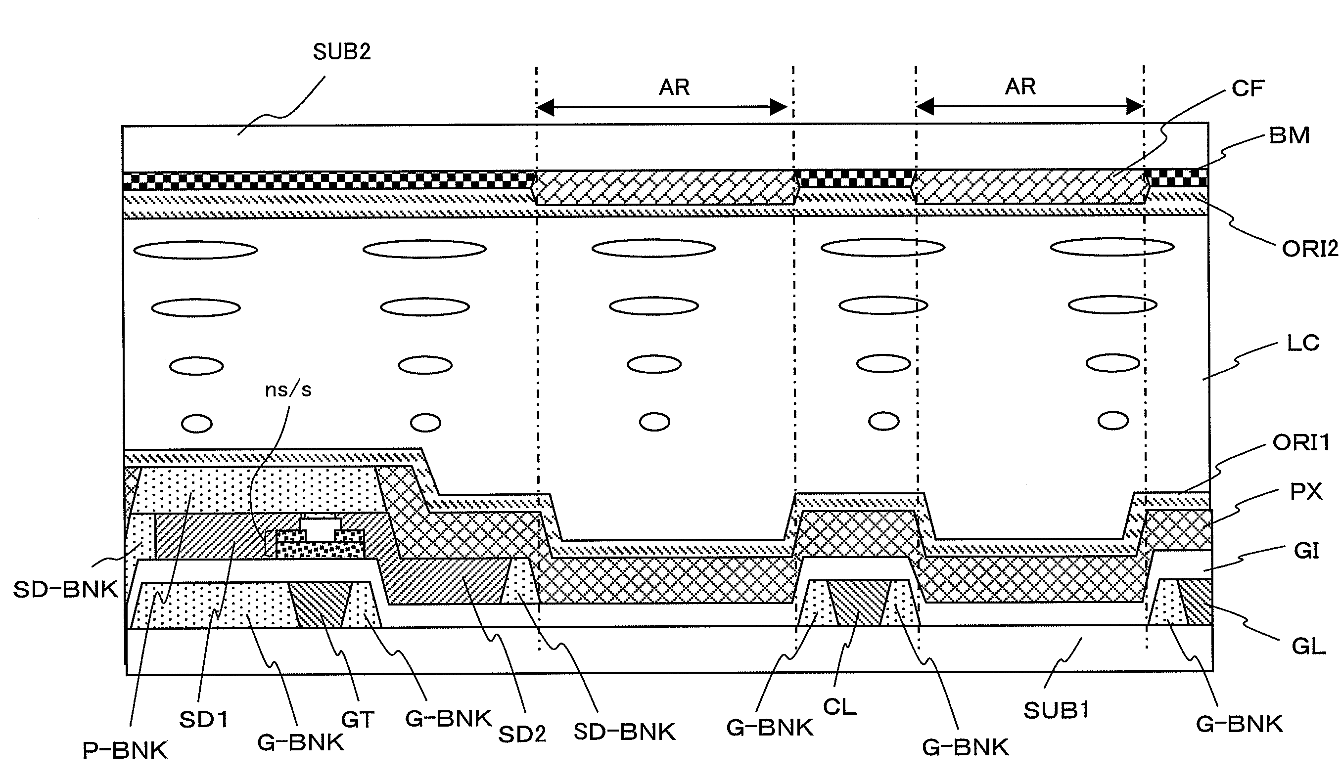
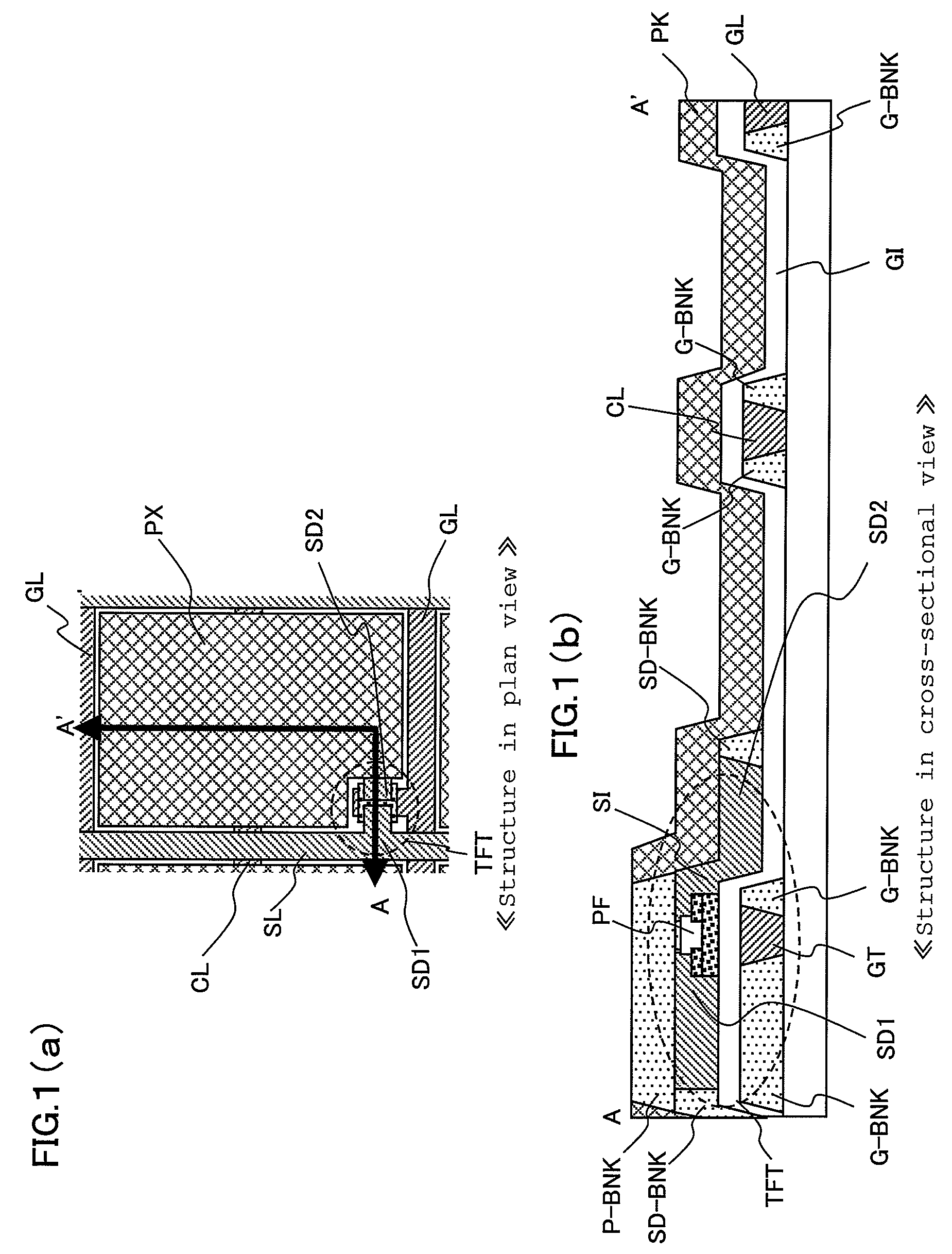
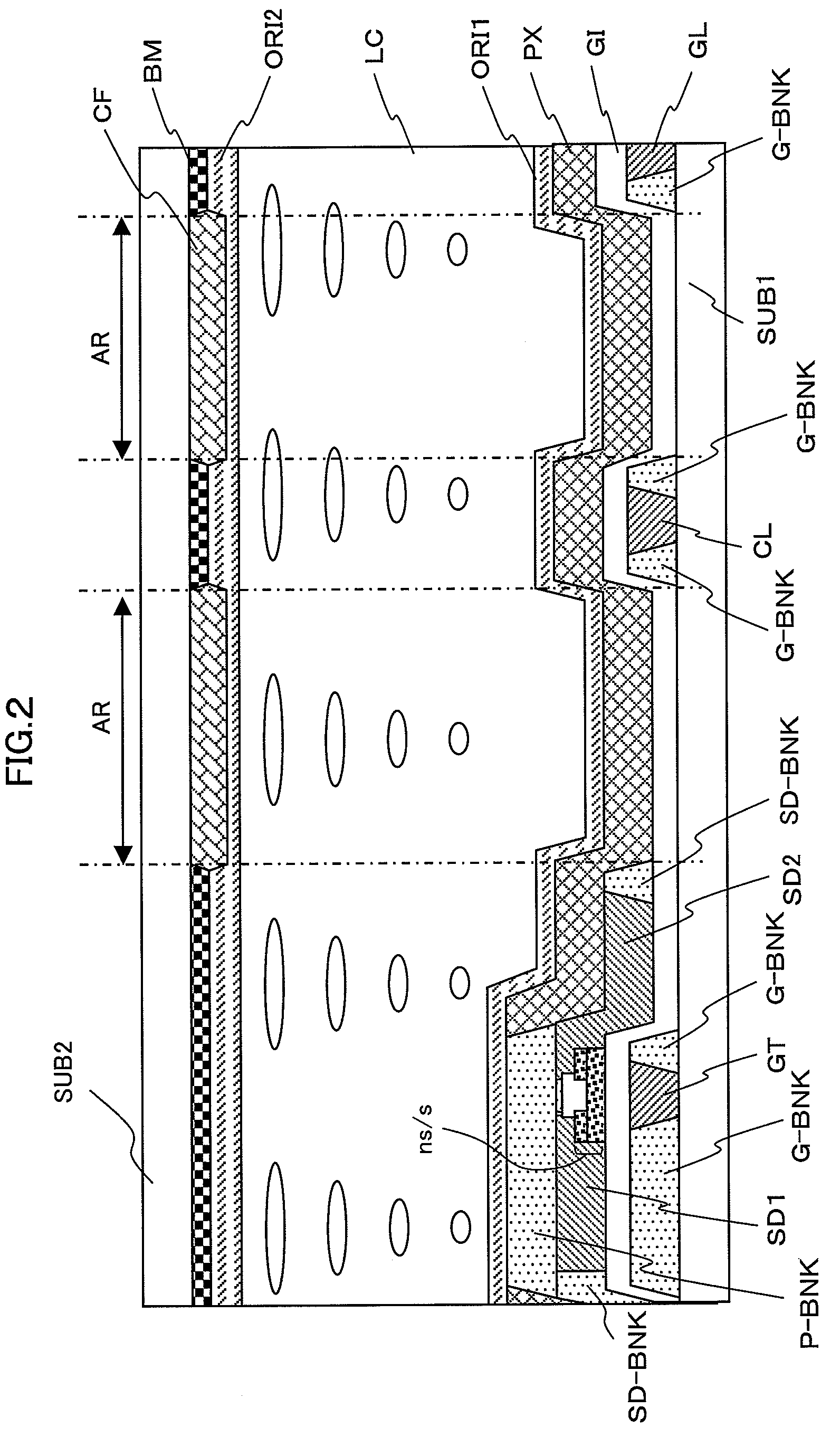
[0057]FIG. 4 represents drawings to explain one pixel of a first substrate (a thin-film transistor substrate) of a liquid crystal display panel of Embodiment 2 of the present invention. FIG. 4(a) is a plan view, and FIG. 4(b) is a cross-sectional view along the line A-A′ in FIG. 4(a). FIG. 5 is a schematical drawing to show cross-section of one pixel of the liquid crystal display panel prepared by attaching a second substrate, i.e. a counter substrate, to the first substrate shown in FIG. 4(b) and by sealing a liquid crystal between the two substrates. To facilitate the explanation, a counter electrode on the second substrate is not shown in FIG. 5. FIG. 6 represents plan views to sequentially explain a process for manufacturing the first substrate in Embodiment 2.

[0058]In FIG. 4, there are provided a plurality of gate lines GL formed on the first substrate SUB1, for which glass is used as a suitable material, and a plurality of source lines SL crossing the gate lines, and one pixel...

embodiment 3

[0069]FIG. 7 represents drawings to explain one pixel of a first substrate (a thin-film transistor substrate) of a liquid crystal display panel of Embodiment 3 for the liquid crystal display device of the present invention. FIG. 7(a) is a plan view, and FIG. 7(b) is a cross-sectional view along the line A-A′ in FIG. 7(a). FIG. 8 is a schematical view showing a cross-section of one pixel of the liquid crystal display panel prepared by attaching a second substrate, i.e. a counter electrode, to the first substrate shown in FIG. 7(b) and by sealing a liquid crystal between the two substrates. To facilitate the explanation, the counter electrode on the second substrate is not shown in FIG. 8. FIG. 9 represents plan views of one pixel for sequentially explaining a process for manufacturing the first substrate of Embodiment 3.

[0070]In FIG. 7, there are provided a plurality of gate lines formed on the first substrate SUB1, for which glass is used as a suitable material, and a plurality of s...

embodiment 4

[0085]FIG. 12 represents drawings to explain one pixel of a first substrate (a thin-film transistor substrate) of a liquid crystal display panel of Embodiment 4 of the present invention. FIG. 12(a) is a plan view, and FIG. 12(b) is a cross-sectional view along the line A-A′ in FIG. 12(a). FIG. 13 is a schematical drawing to show cross-section of one pixel of the liquid crystal display panel prepared by attaching a second substrate, i.e. a counter substrate, to the first substrate shown in FIG. 12(b) and by sealing a liquid crystal between the two substrates. To facilitate the explanation, a counter electrode on the second substrate is not shown in FIG. 13. FIG. 14 represents plan views to sequentially explain a process for manufacturing the first substrate in Example 4.

[0086]The structure of Embodiment 4 is approximately the same as that of Embodiment 3. The pixel electrode PX and the drain electrode SD2 are connected with each other by the separation pattern SPP. It is different fr...


PUM

PropertyMeasurementUnit
temperatureaaaaaaaaaa
conductiveaaaaaaaaaa
shieldingaaaaaaaaaa

Abstract

The present invention provides a liquid crystal display device with high brightness and high display quality manufactured at low cost without causing the decrease in transmissivity. The liquid crystal display device comprises a gate line GL with a gate electrode GT of thin-film transistor prepared on a first substrate SUB1 and used for applying a scan signal, a gate insulator film GI deposited to cover the gate line, a semiconductor layer nS/S formed in island-like shape on the gate insulator film and to constitute an active layer of the thin-film transistor, a source electrode SD1 and a drain electrode SD2 arranged on the gate insulator film and individually connected to said semiconductor layer, and a pixel electrode PX connected to the drain electrode SD2 wherein the gate line GL and the gate electrode GT, the source electrode SD1, the drain electrode SD2, and the pixel electrode PX are prepared by ink jet coating of a conductive solution in a region enclosed by banks G-BNK, SD-BNK, and P-BNK of the insulator film and by baking. Each of these banks is arranged only in a region where it is concealed by the light shielding film BM on the second substrate SUB2.

Description

BACKGROUND OF THE INVENTION[0001]1. Field of the Invention[0002]The present invention relates to a liquid crystal display device. In particular, the invention relates to a liquid crystal display device using an active matrix type liquid crystal display panel.[0003]2. Description of the Prior Art[0004]A liquid crystal display device comprises a liquid crystal display panel, a driving circuit, and peripheral devices such as backlight. A liquid crystal display panel of a typical liquid crystal display device of active matrix longitudinal electric field type (the so-called TN type) is prepared by sealing a liquid crystal between a first panel, which is made up by a first substrate (active matrix substrate or thin-film transistor substrate; TFT substrate) and a second panel made up by a second substrate (counter substrate or color filter substrate).[0005]A new technique to provide a high-performance liquid crystal display panel at low cost is proposed in the Patent Document 1, for instan...

Claims


Application Information

Patent Timeline
Patent Type & Authority Applications(United States)
IPC IPC(8): G02F1/1333
CPCG02F1/133512G02F2001/136295G02F1/136286G02F1/136213G02F1/136295G02F1/136
Inventor ABE, MAKOTOTANAKA, TSUTOMUTSUMURA, MAKOTO
Owner FUTURE VISION
Why Eureka
Try Eureka