

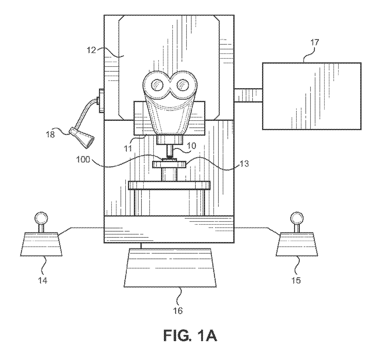
Bond test apparatus and method
a test apparatus and bonding technology, applied in the direction of instruments, mechanical means, force/torque/work measurement apparatus, etc., can solve the problems of low degree of control for users, difficult and expensive process of mounting strain gauges on flexures, and little control over jaw separation, etc., to achieve fewer electrical components, fewer potential errors, and large linear output
- Summary
- Abstract
- Description
- Claims
- Application Information
AI Technical Summary
Benefits of technology
Problems solved by technology
Method used
Image

Examples
first embodiment
[0174]FIG. 6A shows a Hall effect sensor 220 and diametric disk magnet 110, which is suitable for use in the present invention. As described in the summary of invention above, Hall effect sensors provide an output voltage, the magnitude of which depends on the magnetic field experienced at the sensor. Displacement of a magnet relative to the Hall effect sensor therefore creates a change in magnetic field at the sensor, which is shown as a change in the voltage output signal from the Hall effect sensor.
[0175]The Hall effect sensor is arranged to sit adjacent to the magnet, out of the magnet's plane of movement. The sensing face 230 of the Hall effect sensor is arranged to face the magnet, such that displacement of the magnet relative to the sensor causes a change in the magnetic field experienced at the sensing face 230. The north (N) and south (S) poles of the magnet are aligned with the magnet's axis of movement (which is indicated by arrows) in order to maximise the change of magn...
second embodiment
[0176]As shown in FIG. 6B, in a second embodiment two Hall effect sensors 220 are used, with the sensors arranged opposite one another on either side of the magnet 110. By coupling the outputs of the two sensors, the magnitude of the output signal is increased, thus increasing the sensitivity of the apparatus.
[0177]As shown in FIG. 6C, the output voltage signal 250 from the single sensor of FIG. 6A, and the output voltage signal 300 from the dual sensors of FIG. 6B exhibit a highly linear correlation (as indicated by high R2 values) with magnet displacement distance over short distances, for example up to 2 mm (0 to 1.8 mm in FIG. 6C), allowing small displacements to be measured to a high degree of accuracy. The output of even a single Hall effect sensor is also shown to vary by several volts per millimetre, allowing easy measurement without the need to amplify weak voltage signals. This accuracy, and the magnitude of the output signals, makes Hall effect sensors highly suitable for...
PUM
| Property | Measurement | Unit |
|---|---|---|
| voltage | aaaaa | aaaaa |
| voltage | aaaaa | aaaaa |
| voltage | aaaaa | aaaaa |
Abstract
Description
Claims
Application Information