Pixel structure

Active Publication Date: 2019-06-06
AU OPTRONICS CORP
View PDF0 Cites 19 Cited by
  • Summary
  • Abstract
  • Description
  • Claims
  • Application Information

AI Technical Summary

Problems solved by technology

However, when being damaged or falling off, the light-emitting element cannot emit ligh

Method used


Image

  • Pixel structure
  • Pixel structure
  • Pixel structure

Examples


first embodiment

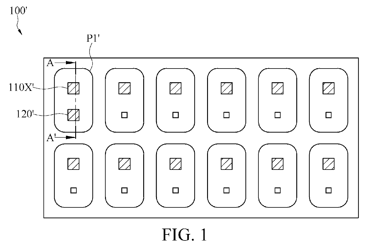
[0022]FIG. 4 is a top view of a pixel structure according to the present disclosure. Referring to FIG. 4, in this embodiment, the pixel structure 100 includes a plurality of sub-pixels P. The plurality of sub-pixels P is arranged in a matrix in a first direction D1 and a second direction D2. A structure of the plurality of sub-pixels can enable a display panel to achieve a full-color display effect. For example, the pixel structure 100 has a first sub-pixel P1 and a second sub-pixel P2 which respectively have a light-emitting element (for example, a first micro light-emitting element 110X). If a detection result shows that a function of the first micro light-emitting element 110X of the first sub-pixel P1 is abnormal (for example, being abnormal in this specification may be luminance degradation or nonluminous, but the present disclosure is not limited thereto), the first micro light-emitting element 110X that has an abnormal function may be reprocessed or repaired. That is, another...

second embodiment

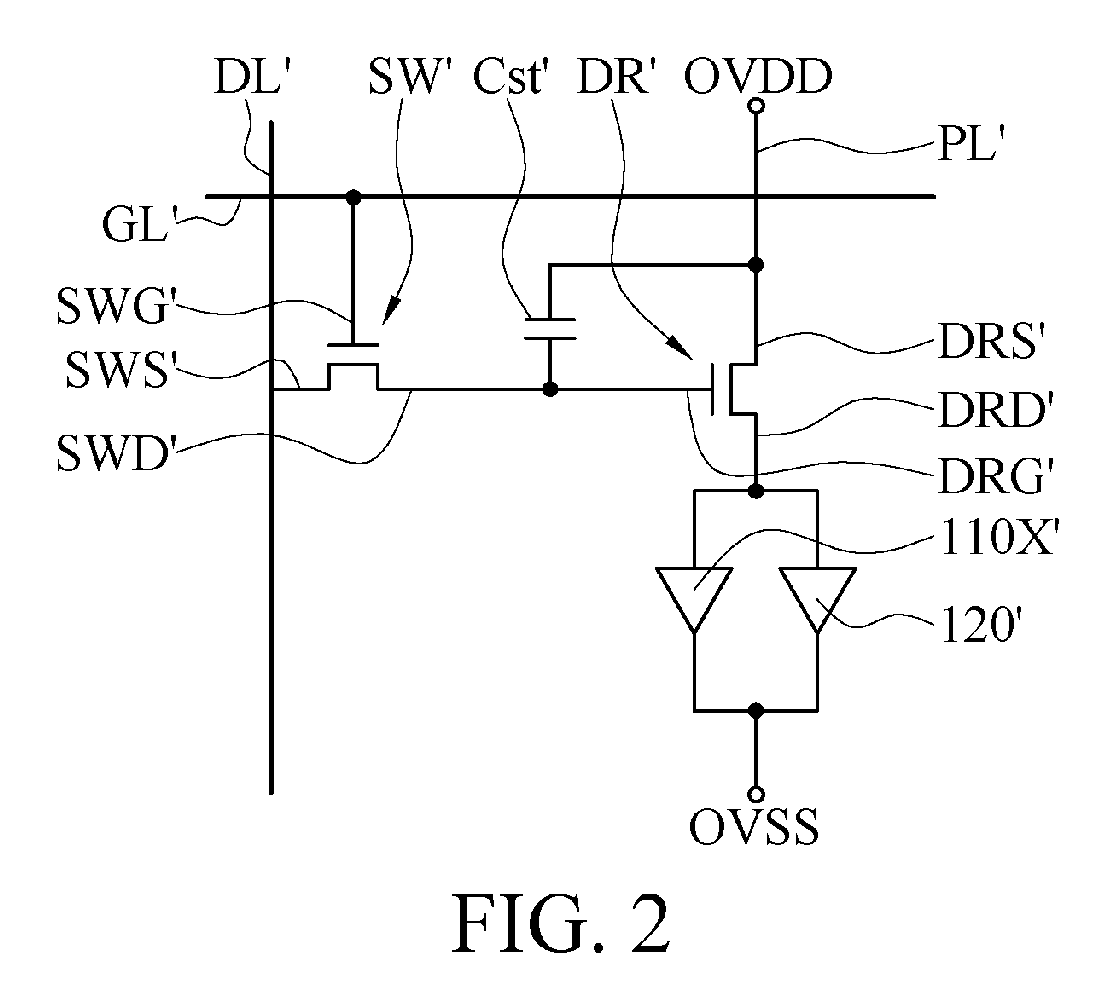
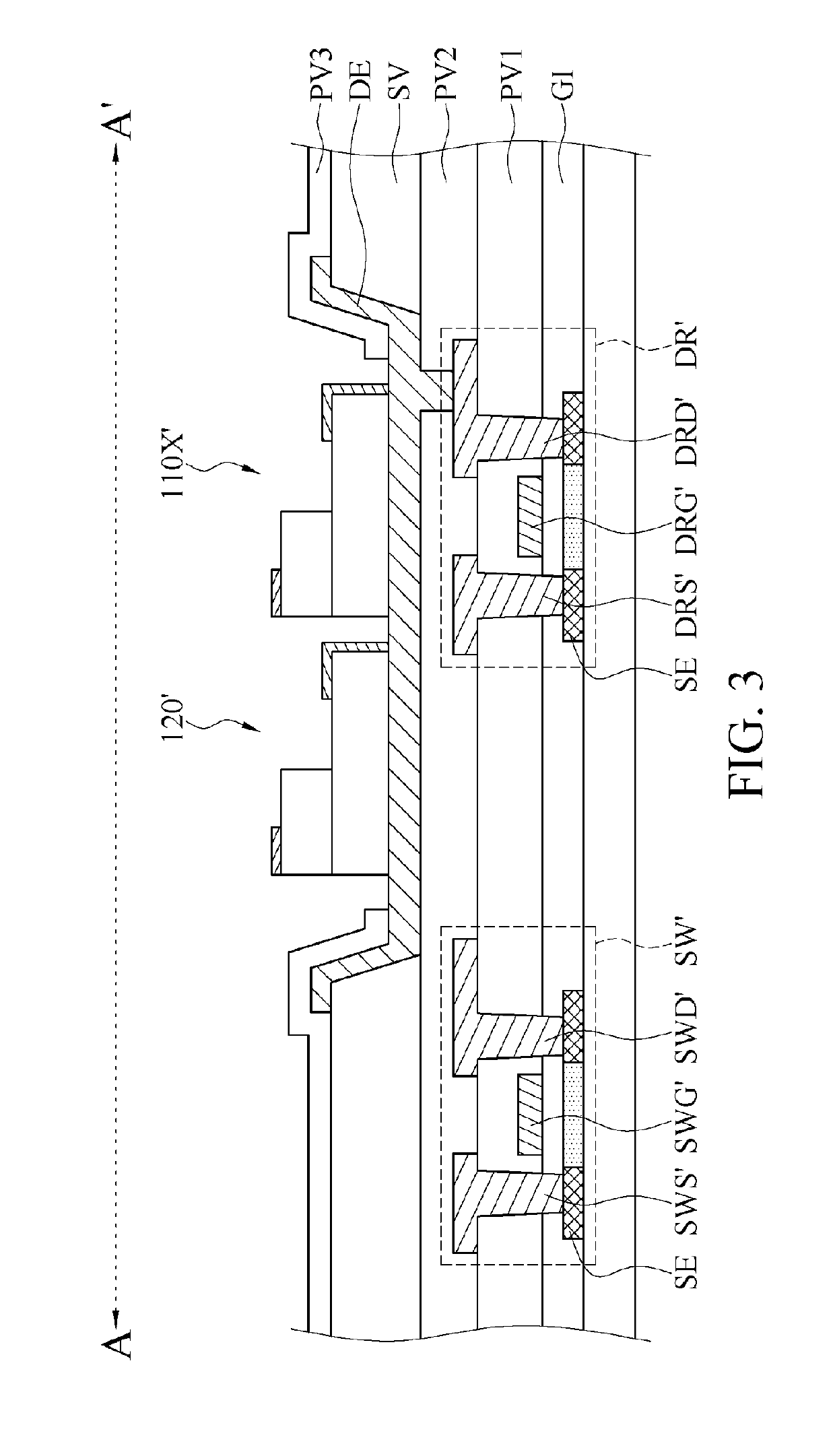
[0053]In another embodiment, the pixel structure 100 includes multiple sub-pixels P, and at least one sub-pixel P may have two light-emitting elements (for example, a first micro light-emitting element 110X and a second micro light-emitting element 190). FIG. 11 is a top view of a pixel structure according to the present disclosure. FIG. 12 is a schematic cross-sectional view of a pixel structure according to an example embodiment along section line C-C′ corresponding to FIG. 11. FIG. 13 is an equivalent circuit diagram of the pixel structure corresponding to FIG. 12. Referring to FIG. 11, FIG. 12, and FIG. 13, it should be noted that, FIG. 12 is a simple schematic diagram, and does not show electrodes of the first micro light-emitting element 110X, the second micro light-emitting element 190, and a repair micro light-emitting element 120, or lines used for electrical connection are not shown (for example, first to fourth electrodes 113, 114, 123, 124, 193, 194, a first connecting l...


PUM


Abstract

A pixel structure includes at least one sub-pixel. The sub-pixel includes a substrate, a first micro light-emitting element, a repair micro light-emitting element, a first connecting line, a second connecting line, and a bridge pattern. The first micro light-emitting element is disposed on the substrate. The repair micro light-emitting element is disposed on the first micro light-emitting element and partially overlaps the first micro light-emitting element in a vertical direction of the substrate. The first connecting line is electrically connected to a first electrode of the first micro light-emitting element and a third semiconductor layer of the repair micro light-emitting element. The second connecting line is electrically connected to a second electrode of the first micro light-emitting element. The bridge pattern is located between the first micro light-emitting element and the repair micro light-emitting element, and is electrically connected to the second electrode and a fourth semiconductor layer of the repair micro light-emitting element.

Description

BACKGROUNDTechnical Field[0001]The present disclosure relates to a sub-pixel repair technology, and in particular, to a pixel structure.Related Art[0002]Light-emitting elements are widely applied to display panels for their advantages such as high photoelectric conversion efficiency and long life-time. Usually, a light-emitting element is disposed in a sub-pixel. However, when being damaged or falling off, the light-emitting element cannot emit light. Consequently, dark spots are generated on the display panel. Further, it is difficult to reprocess the display panel and the process is cumbersome. This is the direction that the industry still endeavors to improve at present.SUMMARY[0003]An embodiment of the present disclosure provides a pixel structure, including a substrate, at least one driving element, a first micro light-emitting element, a repair micro light-emitting element, a first connecting line, a second connecting line, an insulation layer, and a bridge pattern. A driving ...

Claims


Application Information

Patent Timeline
IPC IPC(8): H01L21/66H01L25/075H01L27/12H01L33/62
CPCH01L22/22H01L25/0756H01L27/1214H01L33/62H01L27/15H01L25/0753H01L25/167H01L33/44
Inventor GUO, TING-WEICHANG, CHENG-CHIEHLIN, CHEN-CHILIU, YI-CHENG
Owner AU OPTRONICS CORP
Why Eureka
Try Eureka