Semiconductor device having shared bit line structure and method of manufacturing the same

a technology of semiconductor devices and bit lines, which is applied in the direction of semiconductor devices, semiconductor/solid-state device details, electrical apparatus, etc., can solve the problems of unwanted interactions between adjacent features and closely spaced bit lines, and achieve the effect of reducing photolithographic operations

Active Publication Date: 2010-01-07
SAMSUNG ELECTRONICS CO LTD
View PDF5 Cites 3 Cited by
  • Summary
  • Abstract
  • Description
  • Claims
  • Application Information

AI Technical Summary

Benefits of technology

[0008]It is another feature of an embodiment to provide a method of fabricating a device according to embodiments in which photolithographic operations are reduced.

Problems solved by technology

The high degree of integration results in features, e.g., conductive lines such as bit lines, that are closely spaced together, which may result in unwanted interactions between adjacent features.
For example, closely-spaced bit lines may generate RC delays due to interaction therebetween.

Method used


Image

  • Semiconductor device having shared bit line structure and method of manufacturing the same
  • Semiconductor device having shared bit line structure and method of manufacturing the same
  • Semiconductor device having shared bit line structure and method of manufacturing the same

Examples


first embodiment

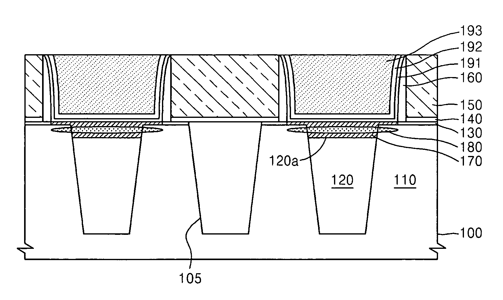
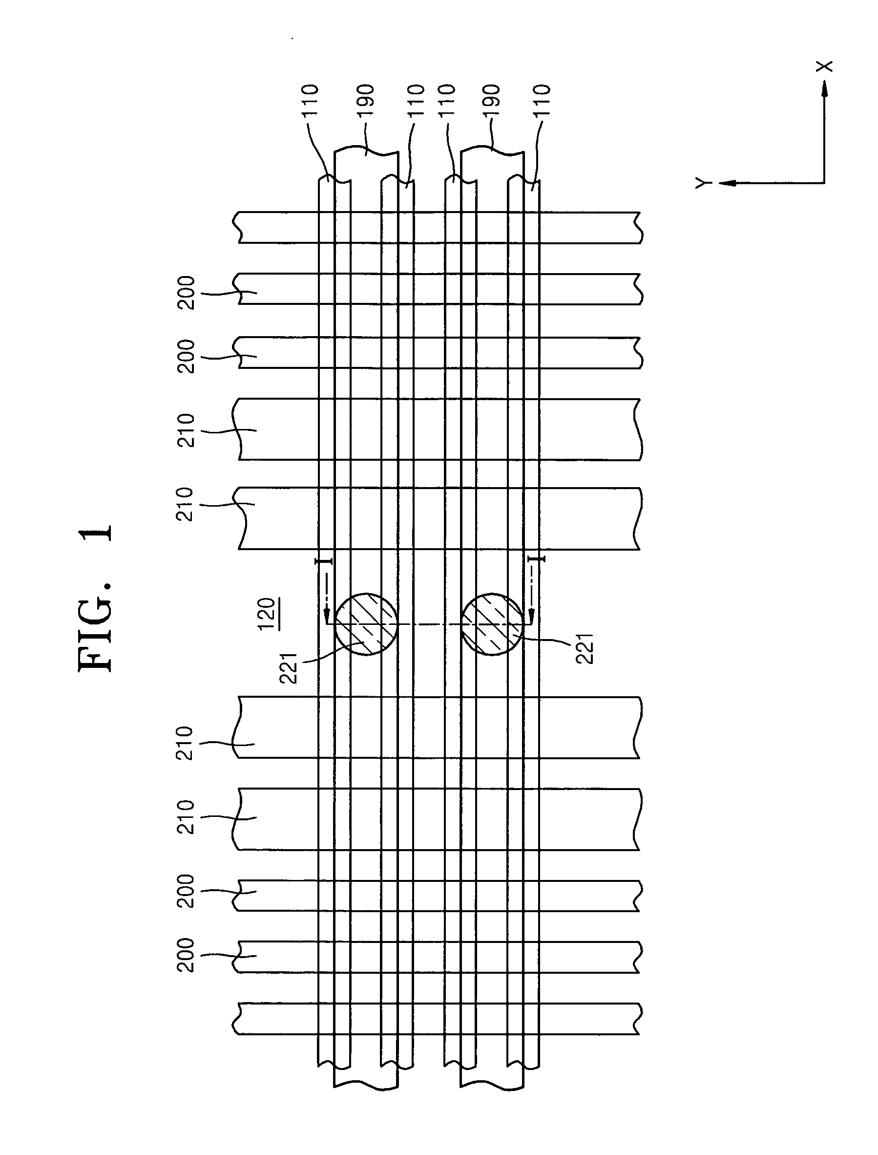
[0058]FIG. 3 illustrates a cross-sectional view of the device of FIG. 1, taken along the line I-I in FIG. 1. Referring to FIG. 3, substrate 100 may include the active regions 110. The active regions 110 may be separated by the field regions 120.

[0059]The field regions 120 may be covered by a first interlayer dielectric (ILD) layer 150. Between the first ILD layer 150 and the underlying substrate 100, a tunneling isolation (tunnel oxide) layer 130 and then a stop layer 140, e.g., a silicon nitride (SiN) stop layer, may be sequentially stacked on the substrate 100.

[0060]An upper surface 120a of the field region 120 may be recessed with respect to an uppermost surface of the substrate 110. The recessed upper surface 120a may thus expose sidewalls of the adjacent active regions 110, thereby providing an increased contact area therewith. A shared bit line contact plug 193 formed of a conductive material, e.g., tungsten, may be on the upper surface 120a of the field region 120 and on the ...

second embodiment

[0067]FIG. 4 illustrates a cross-sectional view of the device of FIG. 1 in which an active bridged region 170 is employed. Referring to FIG. 4, the upper surface 120a of the field region 120 may be recessed with respect to the uppermost surface of the substrate 100, thus exposing sidewalls of the adjacent active regions 110 to provide an increased contact area therewith. The active bridged region 170 may be disposed in the recess, such that the active bridged region 170 extends across the field region 120 and is in contact with the exposed sidewalls of the adjacent active regions 110. Thus, the active bridged region 170 may serve to electrically connect the two adjacent active regions 110.

[0068]The shared bit line contact plug 193 may be disposed on the active bridged region 170. The shared bit line contact plug 193 may be formed of a conductive material such as tungsten, polysilicon, etc.

[0069]In an implementation, the active bridged region 170 may be a polycrystalline silicon laye...

third embodiment

[0070]FIG. 5 illustrates a cross-sectional view of the device of FIG. 1 in which a separated SEG active bridged pattern 170′ is employed. The active bridged region 170′ may include opposing portions 171 and 172, which may be separated by a gap therebetween. The portions 171 and 172 may be formed by SEG. In the SEG process, crystal growth from the laterally opposed sidewalls of the adjacent active regions 110 toward the center of the field region 120 may be stopped before the portions 171 and 172 join.

[0071]In an implementation, the portions 171 and 172 of the active bridged pattern 170′ may be doped using ion implantation to form respective impurity regions 181 and 182.


PUM


Abstract

A semiconductor device, including a substrate having first and second active regions, the first and second active regions being disposed on opposite sides of an isolation structure, and a bit line electrically coupled to a contact plug that is on the isolation structure between the first active region and the second active region, and electrically coupled to an active bridge pattern directly contacting at least one of the first and second active regions, wherein the contact plug is electrically coupled to the first active region and the second active region, and a bottom surface of the active bridge pattern is below a top surface of the first and second active regions.

Description

BACKGROUND[0001]1. Field[0002]Example embodiments relate to a semiconductor device having shared bitline structure and method of manufacturing the same.[0003]2. Description of the Related Art[0004]Advances in semiconductor device design have let to highly integrated devices. The high degree of integration results in features, e.g., conductive lines such as bit lines, that are closely spaced together, which may result in unwanted interactions between adjacent features. For example, closely-spaced bit lines may generate RC delays due to interaction therebetween. Accordingly, there is a need for a device design that reduces or eliminates such unwanted interactions while maintaining a high level of integration. Further, there is a need for a method of manufacturing a highly integrated device that reduces a number of process steps, particularly photolithographic operations.SUMMARY[0005]Example embodiments are therefore directed to providing a semiconductor device having shared bitline st...

Claims


Application Information

Patent Timeline
Patent Type & Authority Applications(United States)
IPC IPC(8): H01L29/06
CPCH01L27/115H01L27/11521H01L27/11519H10B41/10H10B69/00H10B41/30H01L21/28
Inventor JANG, DONG-HOONYOON, YOUNG-BAEKANG, HEE-SOORAH, YOUNG-SEOPCHOE, JEONG-DONG
Owner SAMSUNG ELECTRONICS CO LTD
Why Eureka
Try Eureka