Crack structures, tunneling junctions using crack structures and methods of making same

a crack structure and tunnel junction technology, applied in the field of crack structures, tunneling junctions using crack structures and methods of making same, can solve the problems of crack formation, setting the built-in stress,

Active Publication Date: 2018-12-27
ZEDNA AB
View PDF18 Cites 4 Cited by
  • Summary
  • Abstract
  • Description
  • Claims
  • Application Information

AI Technical Summary

Benefits of technology

[0033]The method enables wafer level production of a large number of devices on one wafer that can either be used in a matrix type system, using the entire wafer, or where the individual devices can be singulated into single sensor elements.

Problems solved by technology

However, it is possible to set the built-in stress such that the crack forms before etching away the sacrificial layer.

Method used


Image

  • Crack structures, tunneling junctions using crack structures and methods of making same
  • Crack structures, tunneling junctions using crack structures and methods of making same
  • Crack structures, tunneling junctions using crack structures and methods of making same

Examples


example

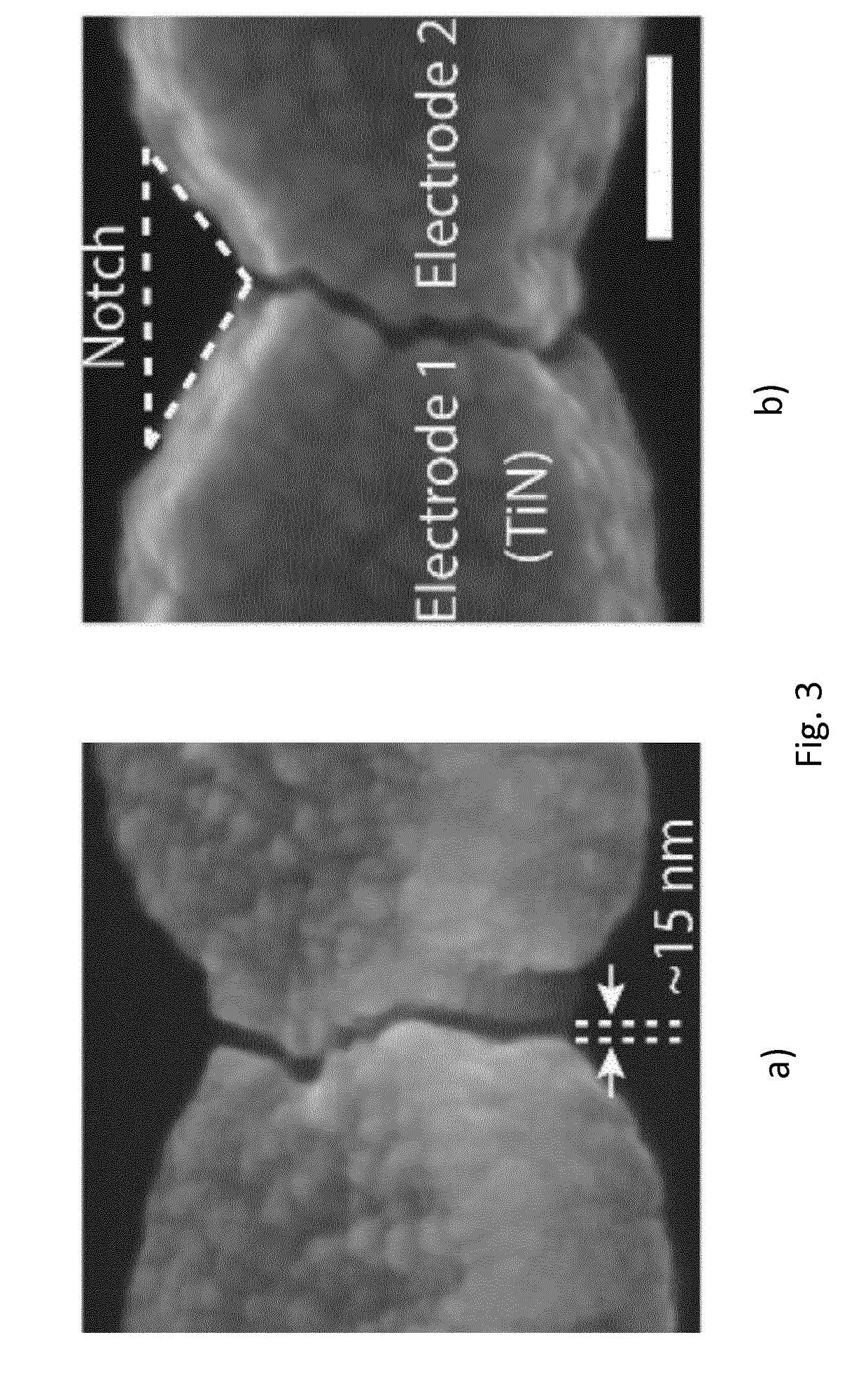
[0049]The crack-junction method is illustrated by the process sequence in FIG. 4. In the crack-junction method, a conductive, suitably metallic, thin film 26, suitably provided between dielectric layers 28, under built-in stress is placed on top of a sacrificial layer 32 on a substrate 34 and patterned to outline a notched 36 electrode bridge as depicted in FIG. 3d. Next, FIG. 4e, the sacrificial material 32 supporting the electrode bridge is selectively removed using isotropic chemical etching, illustrated by arrows. In so doing, the thin film 26 is locally detached from the substrate and the tensile stress that is stored in the thin electrode film is released. This, in turn, causes the build-up of stress in the film at the notch of the electrode bridge. The initiation of a crack at the notch allows contraction of the thin film electrodes in opposite directions, and the formation of a nanoscale gap 38 that is separating the electrodes as illustrated in FIG. 4f. However, it is possi...


PUM

PropertyMeasurementUnit
widthaaaaaaaaaa
widthaaaaaaaaaa
diameteraaaaaaaaaa

Abstract

Disclosed is a method of making a crack structure on a substrate, the crack structure being usable as a tunneling junction structure in a nanogap device, including the controlled fracture or release of a patterned layer under built-in stress, thereby forming elements separated by nanogaps or crack-junctions. The width of the crack-defined nanogap is controlled by locally release-etching the film at a notched bridge patterned in the film. The built-in stress contributes to forming the crack and defining of the width of the crack-defined nanogap. Further, by design of the length of the bridge in a range between sub-μπι to >25μαι, the separation between the elements, defined by the width of the crack-defined nanogaps, can be controlled for each individual crack structure from <2 nm to >100 nm. The nanogaps can be used for tunneling devices in combination with nanopores for DNA, RNA or peptides sequencing.

Description

[0001]The present invention relates to crack structures in or on substrates in general, and in particular to so called crack junctions, usable as electronic nanogaps and tunneling junctions i.a. in devices for DNA sequencing.BACKGROUND OF THE INVENTION[0002]Electronic nanogaps feature rich physics and are fundamental building blocks in a wide range of application areas as described in Dubois, V., Niklaus, F. & Stemme, G. Crack-Defined Electronic Nanogaps. Advanced Materials 28, 2178-2182, doi:10.1002 / adma.201504569 (2016), incorporated herein in its entirety by reference. Nanogap applications can be divided into: (i) applications using electron transport mechanisms such as tunnel junctions and Josephson junctions if superconductive electrodes are employed; (ii) applications using strong light-matter interactions such as plasmonic biosensors; (iii) applications using mechanical tuning of the nanogap width such as nanoelectromechanical switches and mechanically tunable nanophotonics a...

Claims


Application Information

Patent Timeline
Patent Type & Authority Applications(United States)
IPC IPC(8): G01N21/95G01N33/487G01N27/327C12Q1/6869H01L21/66H01L21/302H01L21/02
CPCB82Y5/00B82Y40/00G01N21/9505G01N33/48721G01N27/3278C12Q1/6869H01L22/12H01L21/302H01L21/02603B82Y15/00
Inventor DUBOIS, VALENTINNIKLAUS, FRANKSTEMME, GORAN
Owner ZEDNA AB
Why Eureka
Try Eureka