Array substrate and method of fabricating the same

a technology of array substrate and substrate layer, which is applied in the direction of instruments, semiconductor devices, electrical devices, etc., can solve the problems that the gate insulating layer b>10/b> is also undetectabl

Active Publication Date: 2016-12-27
LG DISPLAY CO LTD
View PDF2 Cites 3 Cited by
  • Summary
  • Abstract
  • Description
  • Claims
  • Application Information

AI Technical Summary

Benefits of technology

[0021]An object of the present invention is to provide an array substrate being capable of addressing disconnection problems related to a connection pattern in a GIP structure array substrate.

Problems solved by technology

In the mask process, a center portion of an ohmic contact layer, which is formed of impurity-doped amorphous silicon, of the semiconductor layer, should be etched by a dry-etching process, however the gate insulating layer 10 is also undesirably etched.

Method used


Image

  • Array substrate and method of fabricating the same
  • Array substrate and method of fabricating the same
  • Array substrate and method of fabricating the same

Examples


second embodiment

[0066]FIG. 6 is a schematic plane view of a non-display region of an array substrate according to the present invention, and FIG. 7 is a cross-sectional view taken along VII-VII line of FIG. 6.

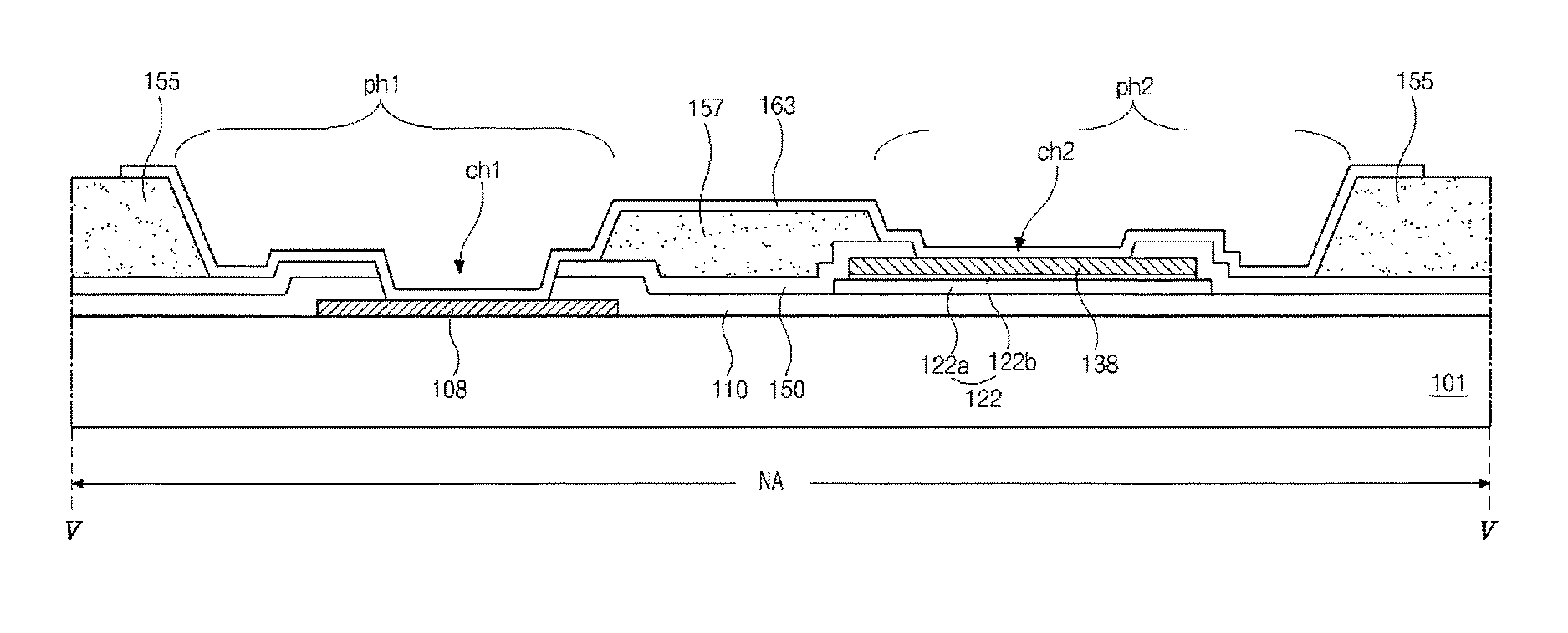
[0067]In the array substrate according to the second embodiment of the present invention, the second auxiliary pattern 138 over the substrate 201 partially overlaps the first auxiliary pattern 108 on the substrate 201. Alternatively, the second auxiliary pattern 138 may completely overlap the first auxiliary pattern 108.

[0068]As shown in FIGS. 6 and 7, the first auxiliary pattern 108 is formed on the substrate 201, and the gate insulating layer 110 is formed on the first auxiliary pattern 108. The second auxiliary pattern 138 is formed over the gate insulating layer 110 to partially overlap the first auxiliary pattern 108. As mentioned above, the second auxiliary pattern 138 may completely overlap the first auxiliary pattern 108. In addition, the second dummy semiconductor pattern 122, which i...

first embodiment

[0076]The other elements in the array substrate have substantially the same structure as those in the array substrate such that the explanations for the other elements are omitted.

third embodiment

[0077]FIG. 8 is a schematic plane view of a non-display region of an array substrate according to the present invention, and FIG. 9 is a cross-sectional view taken along IX-IX line of FIG. 8.

[0078]The array substrate of the third embodiment has a different position for the bridge pattern 157 than that of the second embodiment. According, the following discussion focuses on the bridge pattern 157.

[0079]As shown in FIGS. 8 and 9, in the array substrate of the third embodiment, the bridge pattern 157 partially overlaps the first and second auxiliary patterns 108 and 138. Namely, one end of the bridge pattern 108 overlaps the first auxiliary pattern 108, and the other end of the bridge pattern 138 overlaps the second auxiliary pattern 138.

[0080]In addition, the bridge pattern 157 partially overlaps the first and second contact holes “ch1” and “ch2.” Namely, one end of the bridge pattern 108 is positioned in the first contact hole “ch1,” and the other end of the bridge pattern 138 is pos...


PUM


Abstract

An array substrate according to an embodiment includes a gate line and a data line in a display region and crossing each other to define a pixel region; first and second auxiliary patterns in a non-display region; a gate insulating layer between the gate and data lines and the first and second auxiliary patterns; a passivation layer on the data line and the second auxiliary pattern and including first and second contact holes respectively exposing the first and second auxiliary patterns; a planarization layer on the passivation layer and including first and second pack holes, which respectively correspond to the first and second contact holes; a bridge pattern between the first and second pack holes and overlapping the second auxiliary pattern; a pixel electrode on the planarization layer and in the pixel region; and a connection pattern on the bridge pattern and contacting the first and second auxiliary patterns.

Description

[0001]The present application claims the benefit of Patent Application No. 10-2013-0147303, filed in the Republic of Korea on Nov. 29, 2013, which is hereby incorporated by reference.BACKGROUND OF THE INVENTION[0002]Field of the Invention[0003]The present invention relates to an array substrate, and more particularly, to an array substrate being capable of preventing a disconnection in a jumper portion and a method of fabricating the array substrate.[0004]Discussion of the Related Art[0005]As society has entered the information age, a field of display devices that visually represent all sorts of electrical signals as images has developed rapidly. Particularly, liquid crystal display (LCD) devices or organic light emitting diode (OELD) display devices as a flat panel display device having characteristics of light weight, thinness and low power consumption have been developed for use as a substitute for a cathode-ray tube type display devices.[0006]Since LCD devices include a thin fil...

Claims


Application Information

Patent Timeline
Patent Type & Authority Patents(United States)
IPC IPC(8): H01L27/12
CPCH01L27/124H01L27/1288G02F1/1368H01L29/786H10K50/00H01L27/1262H01L27/1296H01L29/66765
Inventor KIM, JIN-SUUM, SUNG-JINJUNG, JIN-HYUNG
Owner LG DISPLAY CO LTD
Why Eureka
Try Eureka