Thin film-based energy storage devices
a technology of energy storage devices and thin films, applied in the direction of batteries, sustainable manufacturing/processing, final product manufacturing, etc., can solve the problem of compatibility low
- Summary
- Abstract
- Description
- Claims
- Application Information
AI Technical Summary
Benefits of technology
Problems solved by technology
Method used
Image
Examples
embodiment 1
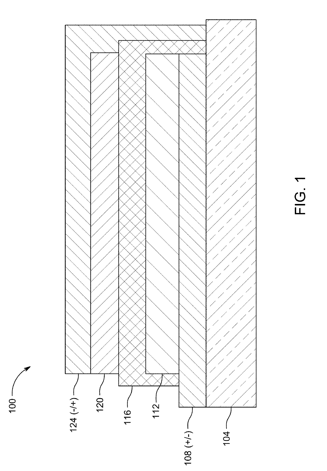
[0289]2. The method of Embodiment 1, wherein printing the current collector layers comprises simultaneously printing the first current collector layer and the second current collector layer.
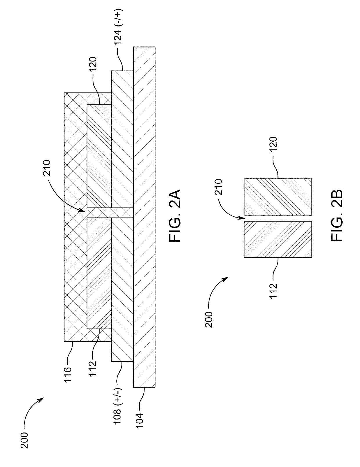
[0290]3. The method of Embodiments 1 or 2, wherein printing the separator comprises simultaneously printing over the exposed surfaces of both of the electrode layers of the first and second types.
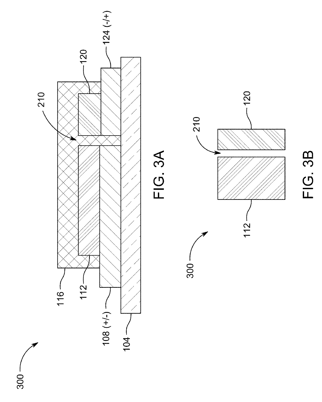
[0291]4. The method of any one of Embodiments 1-3, comprising adjusting a printed area of the electrode layer of the first type and a printed area of the electrode layer of the second type according to the molar ratio.
[0292]5. The method of any one of Embodiments 1-4, wherein printing the separator comprises printing over the exposed surfaces of the electrode layer of the first type prior to printing the electrode layer of the second type, and wherein printing the electrode layer of the second type comprises printing over the separator and over the second current collector layer.
[0293]6. The method of an...
embodiment 7
[0295]8. The method of Embodiment 7, wherein the separator comprises the perforations, wherein the method comprises printing the separator simultaneously over the electrode layers of the first and second types, and wherein the method further comprises one or both of:[0296]printing a further first electrode layer over the separator and over the first electrode, wherein the further first electrode layer fills the perforations in contact therewith, the first electrode layer and the further first electrode layer on opposite sides of the separator and electrically connected to each other; and[0297]printing a further second electrode layer over the separator and over the second electrode, wherein the further second electrode layer fills the perforations in contact therewith, the second electrode layer and the further second electrode layer on opposite sides of the separator and electrically connected to each other.
[0298]9. The method of Embodiment 7, wherein the substrate comprises the pe...
embodiment 10
[0306]11. The method of Embodiment 10, wherein printing the separator comprises simultaneously printing over the exposed surfaces of both of the electrode layers of the first and second types.
[0307]12. The method of Embodiment 10, wherein printing the separator comprises printing over the exposed surfaces of the electrode layer of the first type prior to printing the electrode layer of the second type, and wherein printing the electrode layer of the second type comprises printing over the separator and over the second current collector layer.
[0308]13. The method of any one of Embodiments 1-12, further comprising configuring the first current collector layer as a first current collector having a first polarity and the second current collector layer serves as a second current collector having a second polarity.
[0309]14. The method of any one of Embodiments 1-13, further comprising:[0310]printing a third current collector layer laterally between the first and second current collector l...
PUM
| Property | Measurement | Unit |
|---|---|---|
| voltages | aaaaa | aaaaa |
| thickness | aaaaa | aaaaa |
| thickness | aaaaa | aaaaa |
Abstract
Description
Claims
Application Information


