Pixel structure and touch panel
- Summary
- Abstract
- Description
- Claims
- Application Information
AI Technical Summary
Benefits of technology
Problems solved by technology
Method used
Image

Examples
Embodiment Construction
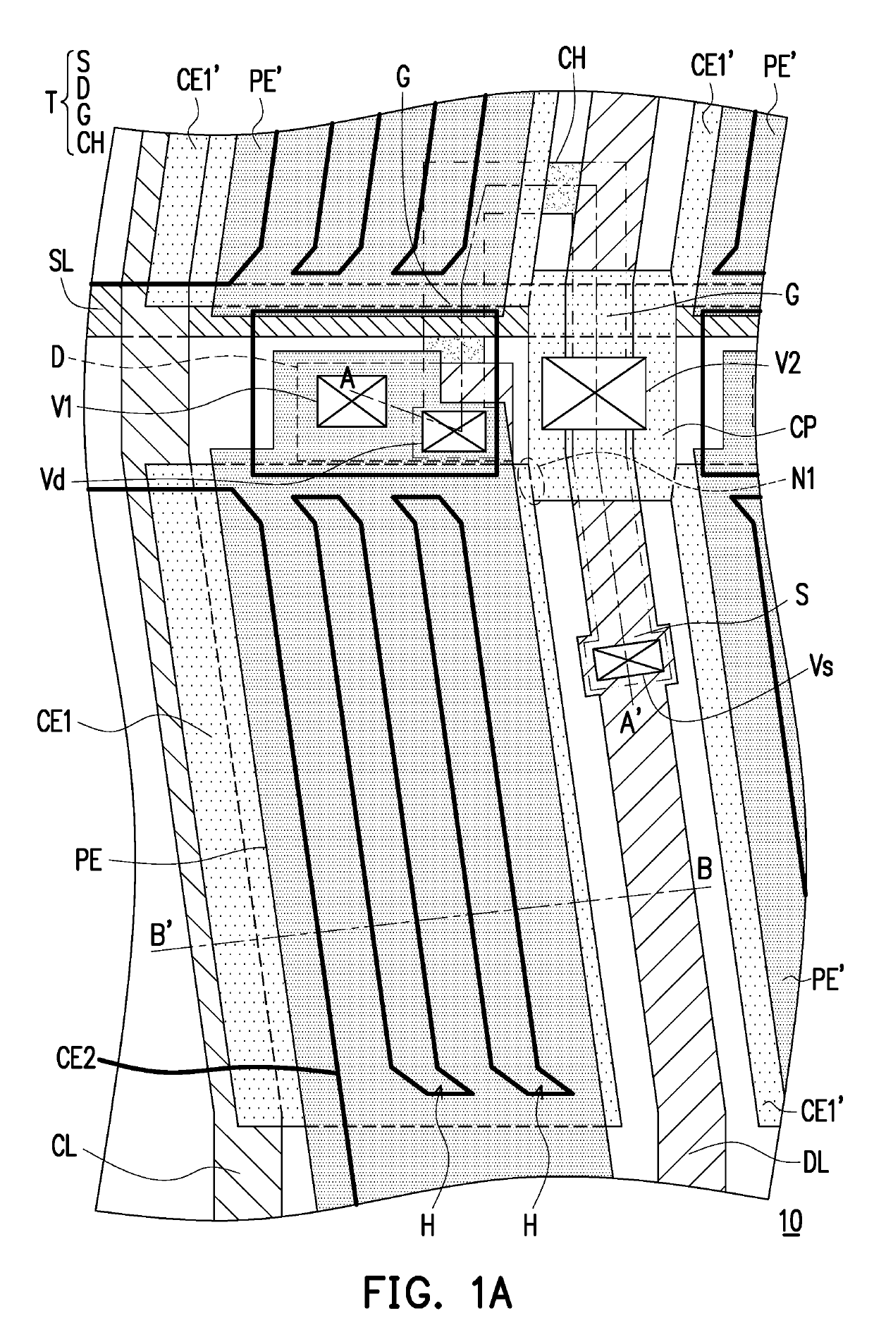
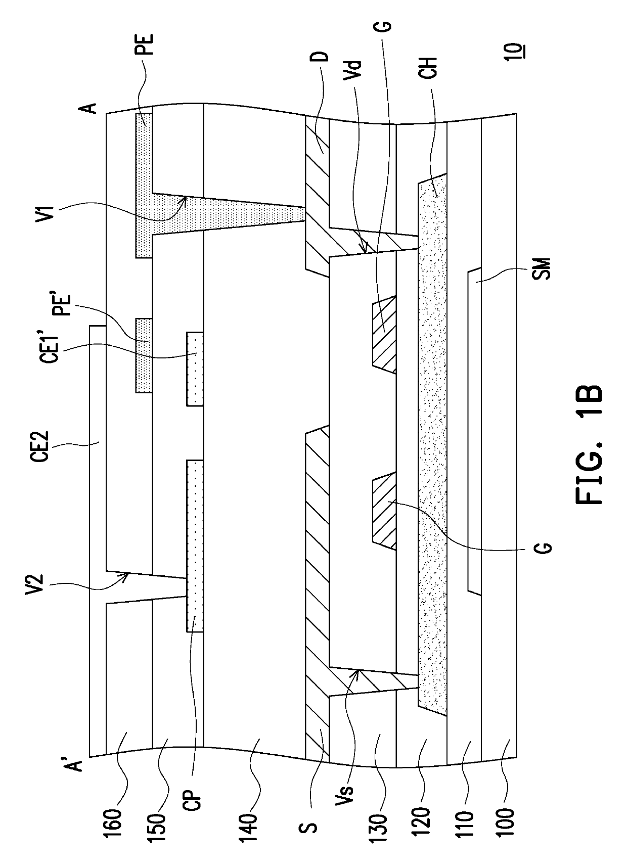
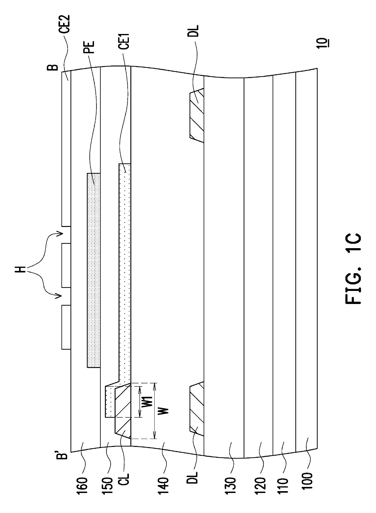
[0017]FIG. 1A is a schematic top view of a pixel structure and its surrounding components in accordance with an embodiment of the present invention. FIG. 1B is a schematic cross-sectional view of a pixel structure according to the section line AN of FIG. 1A. FIG. 1C is a schematic cross-sectional view of a pixel structure according to the section line BB′ of FIG. 1A.
[0018]Please refer to FIGS. 1A to 1C. The pixel structure 10 comprises a scan line SL, a data line DL, a switching element T, a planarization layer 140, a first common electrode CE1, a common line CL, a first insulating layer 150, a pixel electrode PE, a second insulating layer 160, and a second common electrode CE2. In this embodiment, the pixel structure 10 further comprises a substrate 100, a light shielding layer SM, a buffer layer 110, a gate insulating layer 120, and an interlayer dielectric layer 130, but the invention is not limited thereto. In FIG. 1A, three first common electrodes CE1′ and three pixel electrode...
PUM
 Abstract
Description
Claims
Application Information
 - R&D
- Intellectual Property
- Life Sciences
- Materials
- Tech Scout
- Unparalleled Data Quality
- Higher Quality Content
- 60% Fewer Hallucinations
Browse by: Latest US Patents, China's latest patents, Technical Efficacy Thesaurus, Application Domain, Technology Topic, Popular Technical Reports.
© 2025 PatSnap. All rights reserved.Legal|Privacy policy|Modern Slavery Act Transparency Statement|Sitemap|About US| Contact US: help@patsnap.com