Light emitting diode display device

a technology of light-emitting diodes and display devices, which is applied in semiconductor devices, semiconductor/solid-state device details, electrical apparatuses, etc., can solve the problems of high possibility of short-circuit between light-emitting diodes, and achieve the effect of reducing the possibility of short-circuit bumps and improving the yield of display devices

Active Publication Date: 2019-10-03
SAMSUNG ELECTRONICS CO LTD
View PDF1 Cites 2 Cited by
  • Summary
  • Abstract
  • Description
  • Claims
  • Application Information

AI Technical Summary

Benefits of technology

[0005]An aspect of the disclosed embodiments provides a light emitting diode display device which is capable of improving the yield of a display device, by reducing the possibility of short-circuit of bumps for bonding a display board including a light emitting diode and a drive circuit board including a drive transistor.

Problems solved by technology

In a case where the distance between the pixels including the light emitting diodes is narrow, there may be a high possibility of short-circuit between the light emitting diode and a bump for bonding a drive circuit.

Method used


Image

  • Light emitting diode display device
  • Light emitting diode display device
  • Light emitting diode display device

Examples


Embodiment Construction

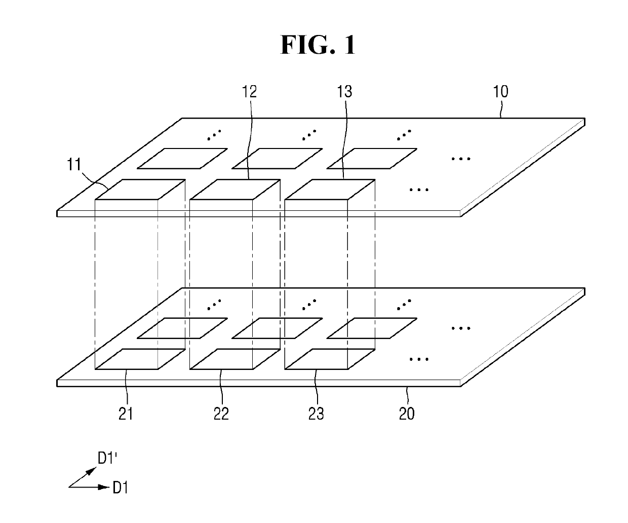
[0024]A light emitting diode display device according to some example embodiments will be described below with reference to FIGS. 1 to 7.

[0025]FIG. 1 is a diagram illustrating a light emitting diode display device according to some example embodiments.

[0026]Referring to FIG. 1, the light emitting diode display device according to some example embodiments may include a display board 10 and a drive circuit board 20.

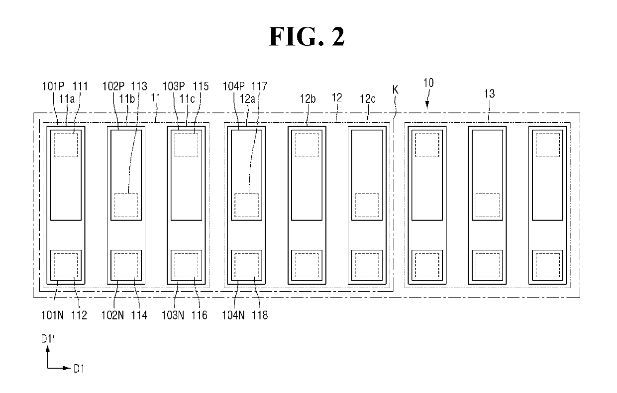
[0027]The display board 10 may include a plurality of unit pixels. Each of the plurality of unit pixels of the display board 10 may be aligned to be spaced apart from each other along a first direction D1 and a first′ direction D1′, which is perpendicular to the first direction D1. The first′ direction′ D1′ may be a direction intersecting with the first direction D1, and on the same horizontal plane. In the drawing, the first direction D1 is illustrated as intersecting with the first′ direction D1′ each other, but the disclosure is not limited thereto. For example, the firs...


PUM


Abstract

A light emitting diode display device includes a display board comprising a plurality of unit pixels, a drive circuit board including a plurality of drive circuit regions corresponding to the plurality of unit pixels, and a plurality of bumps interposed between the plurality of unit pixels and the plurality of drive circuit regions. The plurality of unit pixels comprises a first unit pixel including a first P electrode. The plurality of drive circuit regions comprises a first drive circuit region corresponding to the first unit pixel and a first pad connected to a first drive transistor, the plurality of bumps includes a first solder in contact with the first pad, and a first bump on the first solder and including a first filler in contact with the first P electrode, the first solder includes at least one of tin and silver, and the first filler includes copper or nickel.

Description

[0001]This application claims the benefit of priority under 35 U.S.C. § 119 from Korean Patent Application No. 10-2018-0038440, filed Apr. 3, 2018, in the Korean Intellectual Property Office, the disclosure of which is incorporated herein by reference in its entirety.BACKGROUND1. Field[0002]The present disclosure relates to a light emitting diode display device and, more particularly, to a light emitting diode display device formed on a substrate.2. Description of the Related Art[0003]Recently, the display device has been miniaturized and improved in performance. As a result, a distance between pixels including the light emitting diodes has been narrowed. In a case where the distance between the pixels including the light emitting diodes is narrow, there may be a high possibility of short-circuit between the light emitting diode and a bump for bonding a drive circuit. Further, in a case where the distance between the pixels including the light emitting diode is narrow, the fluidity ...

Claims


Application Information

Patent Timeline
Patent Type & Authority Applications(United States)
IPC IPC(8): H01L33/62H01L25/075H01L27/12H01L23/00
CPCH01L25/0753H01L24/13H01L2224/13139H01L2224/13355H01L33/62H01L2224/13111H01L2924/381H01L2224/13347H01L27/1214H01L27/156H01L25/167H01L2224/0401H01L2224/0603H01L2224/06102H01L2924/12041H01L2224/16227H01L2224/05548H01L2224/13023H01L2224/13082H01L2224/13076H01L2224/13018H01L2224/1403H01L2224/13155H01L2224/13147H01L24/16H01L24/05H01L24/06H01L24/14H01L2224/73253H01L2924/00014H01L2924/014
Inventor SAKONG, TANKIM, YONG ILSEONG, HAN KYUYEON, JI HYELEE, CHUNG SUNHWANG, JI HWAN
Owner SAMSUNG ELECTRONICS CO LTD
Why Eureka
Try Eureka