Composite annular seal and method of making the same

a technology of annular seals and composite materials, applied in the field of seals, can solve the problems of high cost to semiconductor manufacturers, high cost, and high cost of homogenous ffkm seals, and achieve the effects of low cost, high resistance, and convenient splicing

Pending Publication Date: 2020-03-26
PARKER HANNIFIN CORP
View PDF0 Cites 0 Cited by
  • Summary
  • Abstract
  • Description
  • Claims
  • Application Information

AI Technical Summary

Benefits of technology

[0005]Provided herein is a lower cost process chamber seal for semiconductor applications that is highly resistant to aggressive chemical and thermal conditions and a method of manufacturing the same. A composite annular seal having an inner core layer including a first, lower cost elastomeric material and an outer sleeve layer including a second, different elastomeric material is, therefore, provided. The composite annular seal of the present invention may be manufactured by sequential or crosshead co-extrusion of the first elastomeric material and the second elastomeric material to form a radially layered cord having the inner core layer and the outer sleeve layer. After the first elastomeric material of the inner core layer and the second elastomeric material of the outer sleeve layer are co-extruded to form a radially layered cord, the materials are co-cured and crosslinked together at their interface. The co-extruded radially layered cord is then spliced at its ends to form the composite annular seal. The splicing may be facilitated using a small amount of uncured second elastomeric material and curing the small amount of second elastomeric material to secure the ends together and form the composite annular seal. The first elastomeric material may be a fluoroelastomer (FKM) and the second elastomeric material may be a perfluoroelastomer (FFKM).

Problems solved by technology

Homogenous FFKM seals, however, are typically quite expensive and may require replacement on a regular basis as they get etched by the process gases during use, resulting in very high cost to the semiconductor manufacturer.
Moreover, homogenous FFKM seals are somewhat lacking in the level of resilience that is desired for semiconductor sealing applications.

Method used


Image

  • Composite annular seal and method of making the same
  • Composite annular seal and method of making the same

Examples


Embodiment Construction

[0026]Embodiments of the present invention will now be described with reference to the drawings, wherein like reference numerals are used to refer to like elements throughout. It will be understood that the figures are not necessarily to scale. These drawings and this description are not to be construed as being limited to the particular illustrative forms of the invention disclosed. It will become apparent to those skilled in the art that various modifications of the embodiments herein can be made without departing from the spirit or scope of the invention.

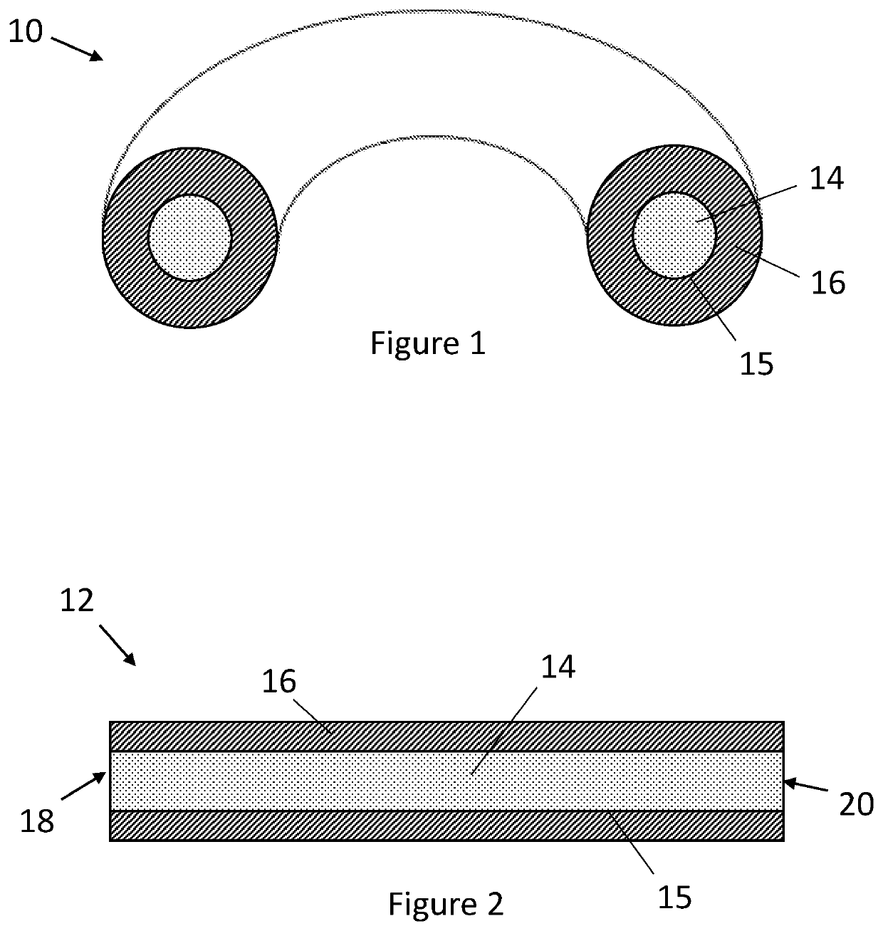
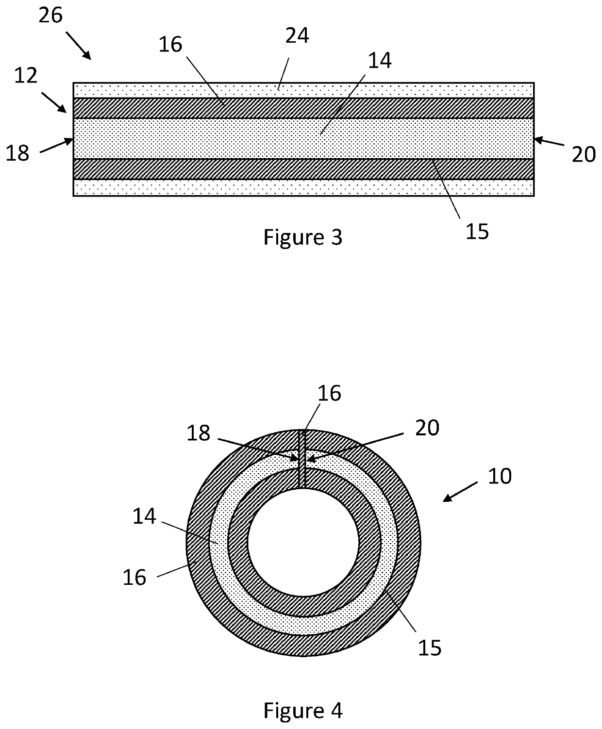
[0027]With reference to FIG. 1, a composite annular seal 10 for sealing a process chamber in a semiconductor is depicted in an axial cross-sectional perspective view.

[0028]The composite annular seal 10 may be, for example, an O-ring seal. The composite annular seal 10 includes a radially innermost core layer 14 (hereinafter referred to as inner core 14) and a radially outermost sleeve layer 16 (hereinafter referred to as outer la...


PUM

PropertyMeasurementUnit
diameteraaaaaaaaaa
diameteraaaaaaaaaa
interior diameteraaaaaaaaaa

Abstract

A method of manufacturing a composite annular seal for a semiconductor process chamber is provided. The method includes extruding a first elastomeric material in uncured form to form a cord of uncured first elastomeric material and extruding, via crosshead extrusion, a second elastomeric material in uncured form onto an outer surface of the cord of uncured first elastomeric material to form an uncured radially layered cord. The uncured radially layered cord includes an inner core of the first elastomeric material and an outer layer of the second elastomeric material. The second elastomeric material is different than the first elastomeric material. The method also includes co-curing the first and second elastomeric material of the uncured radially layered cord to form a cured radially layered cord. The method also includes splicing, via hot vulcanization, a first and second end of the cured radially layered cord to form the composite annular seal.

Description

[0001]This application claims priority to U.S. Provisional Application No. 62 / 733,757 filed Sep. 20, 2018, which is incorporated herein by reference.FIELD OF INVENTION[0002]The present invention relates generally to seals, and more particularly to a composite annular seal having enhanced thermal and chemical resistance for use in a semiconductor process chamber.BACKGROUND OF THE INVENTION[0003]A semiconductor process chamber commonly includes a container, a lid, and a seal that seals an interface between the container and the lid. For example, a continuous annular thermosetting or thermoplastic rubber seal may be used. A common configuration of an annular seal is an O-ring seal having a circular circumference and a circular cross-section, however other annular seals may have a non-circular circumference and / or a non-circular cross-section.[0004]Many semiconductor manufacturing methods now use processing chambers to create ultra-high-vacuum (UHV—pressures lower than about 10−7 pascal...

Claims


Application Information

Patent Timeline
Patent Type & Authority Applications(United States)
IPC IPC(8): B29C48/00B29C48/21
CPCB29C48/21B29L2031/26B29C48/0021B29K2027/12B29C48/022B29C48/06B29C48/154B29C48/34B29C48/91
Inventor BALLARD, JACOBHOWARD, AARON
Owner PARKER HANNIFIN CORP
Why Eureka
Try Eureka