Unit pixel of image sensor and light-receiving element thereof

a technology of image sensor and unit pixel, which is applied in the direction of electrical equipment, semiconductor devices, radio frequency control devices, etc., can solve the problems of generating fixed-pattern noise, physical limitation of enlarge the light-receiving area of the cmos image sensor, and the electrostatic capacity of the photodiode used mainly as the light-receiving unit of the image sensor is relatively small, so as to achieve small electrostatic capacity and less noise. ,

Active Publication Date: 2020-04-16
KIM HOON
View PDF1 Cites 0 Cited by
  • Summary
  • Abstract
  • Description
  • Claims
  • Application Information

AI Technical Summary

Benefits of technology

Since the PPS is generally composed of a single photodiode and a single selection transistor, the PPS has advantageous effects of increasing the aperture ratio and growing the fill factor, which is related to the light-receiving efficiency compared with the APS, which requires three to five MOS transistors for an identical pixel size.
[0007]On the contrary, the PPS has photocurrent with low intensity and converts the photosignal into the form of current, which is vulnerable to the external environment such as noise to use for signal processing, which accounts for its disadvantageous effect of generating fixed-pattern noise (FPN).
[0008]Therefore, for an identical size of the pixel, the APS can obtain the image signal which has less noise than that of the PPS because the APS has a plurality of the transistors in its unit pixel, although the light-receiving unit of the APS gets smaller than that of the PPS in terms of the size of the light-receiving unit.
[0009]Meanwhile, an electron-hole pair (EHP) is generated against a photon incident from the light-receiving unit of the unit pixel of the image sensor while the generated electrons and holes are accumulated in the photodiode, which is the light-receiving unit.
[0010]The maximum electrostatic capacity that can be accumulated in the photodiode is proportional to its light-receiving area. In particular, it is physically limited to enlarge the light-receiving area of the CMOS image sensor in that the CMOS image sensor has an area for arranging the transistors accompanying the CMOS sensor larger than that of the CCD image sensor. In the meantime, the photodiode used mainly as the light-receiving unit of the image sensor has relatively small electrostatic capacity, and therefore, is easily saturated and not easily subdivided in an analog way.
[0011]As a result, the unit pixel of the CMOS image sensor requires a relatively long period for accumulating photocharges so as to generate the minimum charge for processing signals through the limited light-receiving area. Thus, the unit pixel having such a light-receiving unit is not suitable for the image sensor with a high-density / high-speed frame.The band gap of silicon semiconductors is 1.12 eV and such silicon semiconductors can detect light energy of which wavelength ranges from 400 to 1,100 nm when used as the light-receiving element. In other words, such silicon semiconductors cannot detect light of which wavelength is 400 nm or less or 1,100 nm or more and are not applied to any sensors for biometrics, motion recognition and the like, which make use of near infrared or infrared rays, despite their economic efficiency.SUMMARY

Problems solved by technology

On the contrary, the PPS has photocurrent with low intensity and converts the photosignal into the form of current, which is vulnerable to the external environment such as noise to use for signal processing, which accounts for its disadvantageous effect of generating fixed-pattern noise (FPN).
In particular, it is physically limited to enlarge the light-receiving area of the CMOS image sensor in that the CMOS image sensor has an area for arranging the transistors accompanying the CMOS sensor larger than that of the CCD image sensor.
In the meantime, the photodiode used mainly as the light-receiving unit of the image sensor has relatively small electrostatic capacity, and therefore, is easily saturated and not easily subdivided in an analog way.
Thus, the unit pixel having such a light-receiving unit is not suitable for the image sensor with a high-density / high-speed frame.
In other words, such silicon semiconductors cannot detect light of which wavelength is 400 nm or less or 1,100 nm or more and are not applied to any sensors for biometrics, motion recognition and the like, which make use of near infrared or infrared rays, despite their economic efficiency.

Method used


Image

  • Unit pixel of image sensor and light-receiving element thereof
  • Unit pixel of image sensor and light-receiving element thereof
  • Unit pixel of image sensor and light-receiving element thereof

Examples


Embodiment Construction

[0056]Embodiments according to the present disclosure will be described in more detail hereinafter with reference to the accompanying drawings. In describing the present disclosure, any known technique will not be described in detail when it is determined such description can unnecessarily make the subject matter of the present disclosure obscure. Any number used in describing the present disclosure such as a first, a second and the like is nothing but an identifier for distinguishing one element from another one.

[0057]In addition, in the present Specification, when it is specified one element “is connected to” or “comes in contact with” another one, whereas the former element can be directly connected to or come in contact with the latter, it should be understood the two are possibly connected or come in contact with each other with still another element in between as a medium unless otherwise contradictorily specified.

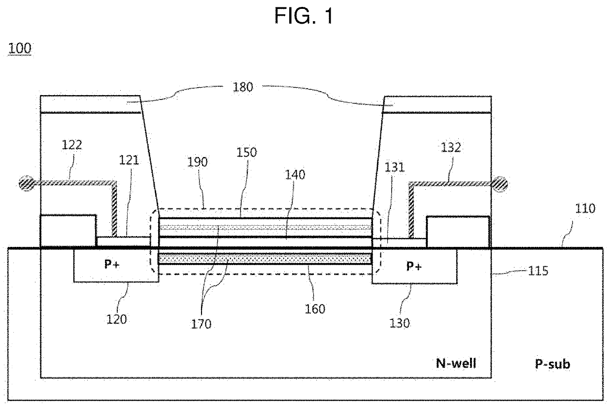
[0058]FIG. 1 is a cross-sectional view of the tunnel junction l...


PUM

PropertyMeasurementUnit
band gapaaaaaaaaaa
wavelengthaaaaaaaaaa

Abstract

Provided are a light-receiving element which has more capability of detecting wavelengths than that of existing silicon light-receiving elements and a unit pixel of an image sensor by using it. The light-receiving element includes: a light-receiving unit which is floated or connected to external voltage and absorbs light; an oxide film which is formed to come in contact with a side of the light-receiving unit; a source and a drain which stand off the light-receiving unit with the oxide film in between and face each other; a channel which is formed between the source and the drain and forms an electric current between the source and the drain; and a wavelength expanding layer which is formed in at least one among the light-receiving unit, the oxide film and the channel and forms a plurality of local energy levels by using strained silicon.

Description

CROSS-REFERENCE TO RELATED APPLICATION[0001]This application is a divisional of U.S. patent application Ser. No. 15 / 885,757, filed Jan. 31, 2018.1. TECHNICAL FIELD[0002]The present disclosure relates to a unit pixel of an image sensor and a light-receiving element thereof, more particularly to a light-receiving element with expanded light-absorbing wavelengths by splitting energy levels of silicon and a unit pixel of an image sensor using the light-receiving element.2. DESCRIPTION OF THE RELATED ART[0003]An image sensor converts an optical signal into an image signal, which, when light is radiated onto a light-receiving unit inside a unit pixel of an image sensor chip, detects the light and its quantity incident upon each of the unit pixels, thereby converting a photosignal to generate an electrical signal and then transfers the electrical signal to an analog circuit unit and a digital circuit unit to form an image.Existing image sensors can be categorized largely into charged coupl...

Claims


Application Information

Patent Timeline
Patent Type & Authority Applications(United States)
IPC IPC(8): H01L31/113H01L31/0232H01L27/146H01L31/036
CPCH01L27/1461H01L31/02327H01L27/14679H01L31/02322H01L31/036H01L31/113H01L27/146H01L31/1136
Inventor KIM, HOON
Owner KIM HOON
Why Eureka
Try Eureka