OLED display panel and photomask

a technology of light-emitting diodes and display panels, applied in the field of display technologies, can solve problems such as non-uniform and achieve the effect of avoiding the feed-through effect and uniformity in displaying images

Active Publication Date: 2020-06-11
WUHAN CHINA STAR OPTOELECTRONICS SEMICON DISPLAY TECH CO LTD
View PDF0 Cites 0 Cited by
  • Summary
  • Abstract
  • Description
  • Claims
  • Application Information

AI Technical Summary

Benefits of technology

[0038]The OLED display panel of the present application includes the plurality of pixel areas, each of which is defined by the electrode and the organic light emitting material. The pixel areas increase in size along the first direction (i.e., the scan driving direction) and the pixel areas increase in size along the second direction (i.e., the data driving direction) perpendicular to the first direction. Accordingly, the present application avoids the feed-through effect caused in transmitting signals using the scan lines and the data lines, thereby achieving uniformity in displaying images.

Problems solved by technology

In a situation that the pixel areas 3 have the same size, the feed-through effect will affect current intensity generated by the EL device in light emission and cause non-uniformity in displaying images.

Method used


Image

  • OLED display panel and photomask
  • OLED display panel and photomask

Examples


Embodiment Construction

[0043]To make the objectives, technical schemes, and effects of the present application more clear and specific, the present application is described in further detail below with reference to the embodiments in accompanying with the appending drawings. It should be understood that the specific embodiments described herein are merely for explaining the present application, the term “embodiment” used in the context means an example, instance, or illustration, and the present application is not limited thereto.

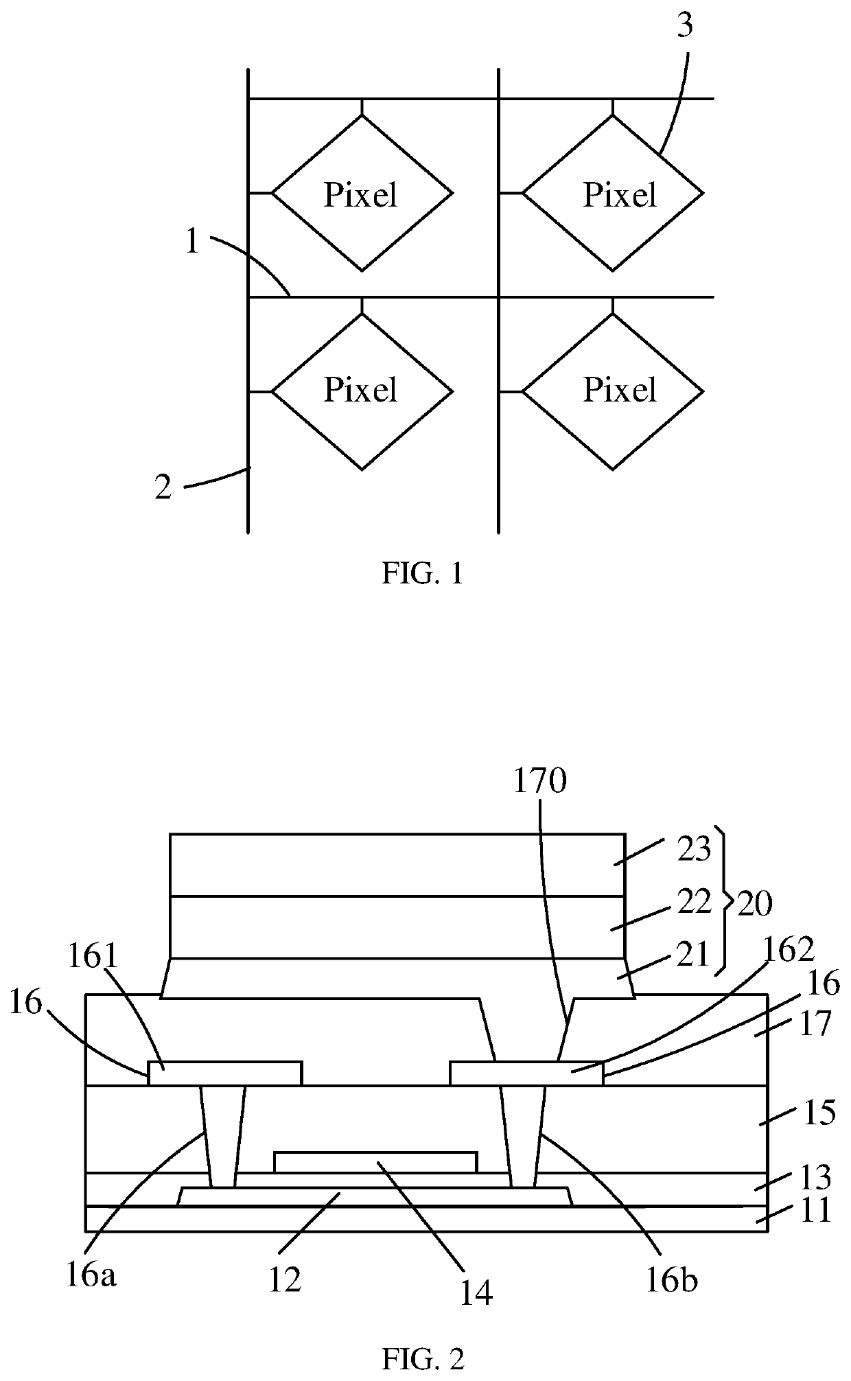
[0044]FIG. 2 is a schematic diagram partially showing an organic light emitting diode (OLED) display panel according to the present application. The OLED display panel includes a thin-film transistor (TFT) array substrate and organic electroluminescence (EL) devices 20 disposed on the TFT array substrate. The TFT array substrate includes a substrate 11, a polycrystalline silicon layer 12, a first insulating layer 13, a gate electrode layer 14, a second insulating layer 15, a sour...


PUM

PropertyMeasurementUnit
sizeaaaaaaaaaa
electric fieldaaaaaaaaaa
resistanceaaaaaaaaaa

Abstract

An OLED display panel and a photomask are provided. The OLED display panel includes a plurality of pixel areas arranged in a matrix on a plane. Each of the pixel areas is defined by an electrode and an organic light emitting material. The pixel areas increase in size along a first direction and the pixel areas increase in size along a second direction perpendicular to the first direction. The application solves the problem of non-uniformity in displaying images, caused by a feed-through effect in existing arts.

Description

FIELD OF DISCLOSURE[0001]The present application relates to display technologies, and more particularly, to an organic light emitting diode (OLED) display panel and a photomask.DESCRIPTION OF RELATED ART[0002]In an OLED display panel, every one of pixel structures includes an organic electroluminescence (EL) device including an anode, a cathode, and a light emitting layer disposed between the anode and the cathode. The light emitting layer is driven by an electric field between the anode and the cathode and emits light rays by injection and recombination of charge carriers.[0003]FIG. 1 is a schematic diagram showing an existing OLED display panel. As shown in FIG. 1, the OLED display panel includes a plurality of scan lines 1, a plurality of data lines 2, and a plurality of pixel areas 3 interlaced by the scan lines 1 and the data lines 2. In the existing art, the pixel areas 3 have a same size. The scan lines 1 and the data lines 2 are metal lines. The resistance of a metal line in...

Claims


Application Information

Patent Timeline
Patent Type & Authority Applications(United States)
IPC IPC(8): H01L27/32H01L51/52
CPCH01L51/5209H01L27/3248H01L27/326H10K59/352H10K59/12H10K59/131H10K59/121H10K50/813H10K59/123
Inventor ZHAO, KAIXIANG
Owner WUHAN CHINA STAR OPTOELECTRONICS SEMICON DISPLAY TECH CO LTD
Why Eureka
Try Eureka