Full-screen display panel

a display panel and full-screen technology, applied in the field of display, can solve the problems of insufficient conventional chip on panel (cop) method of ics being disposed on a lower area of the display panel, and users of the mobile phone will be ups

Inactive Publication Date: 2020-07-09
WUHAN CHINA STAR OPTOELECTRONICS SEMICON DISPLAY TECH CO LTD
View PDF5 Cites 0 Cited by
  • Summary
  • Abstract
  • Description
  • Claims
  • Application Information

AI Technical Summary

Benefits of technology

[0022]The present invention provides a full-screen display panel including a main display section, and at least two COP circuit sections disposed on different lateral sides of the main display section respectively. The main display section and the COP circuit sections are disposed on a flexible substrate, and each of the COP circuit sections is bent rearwardly from one edge of the main display section to a backside of the main display section, thereby making each of the COP circuit sections attached to the backside of the main display section. Furthermore, the present invention provides a full-screen display panel with sufficient edge regions for setting external compensation circuits and drive chips, thereby realizing the full-screen display panel with diverse functions.
[0023]The detailed description of the present nvention and the accompanying drawings are to be understood, instead of limiting thereto.

Problems solved by technology

Taking a mobile phone as an example, if the overall size of the mobile phone is large but the actual display area of the mobile phone is small, users of the mobile phone will be upset as if they were moving from a big house to a small house.
The conventional chip on panel (COP) method that the ICs are only disposed on a lower area of a display panel is no longer sufficient.

Method used


Image

  • Full-screen display panel
  • Full-screen display panel

Examples


Embodiment Construction

[0028]In order to further clarify the technical means and effects of the present invention, the following detailed description will be made in conjunction with the preferred embodiments of the present invention and the accompanying drawings.

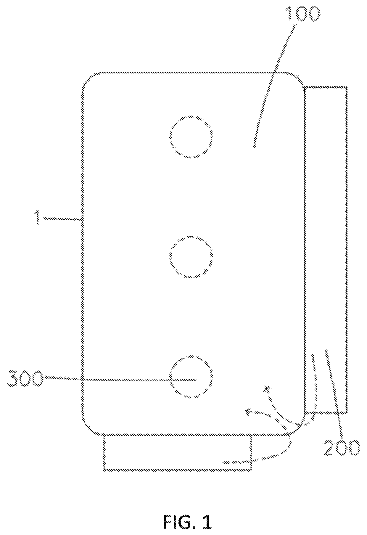
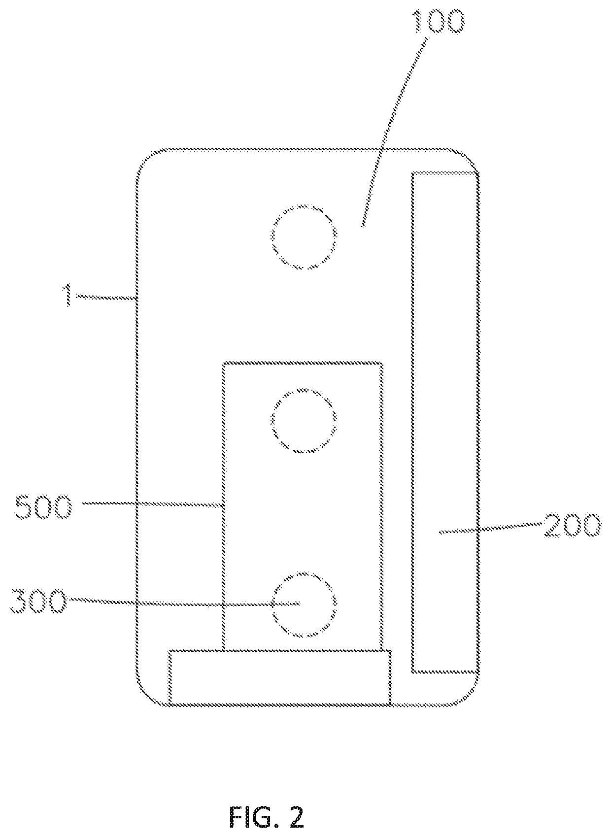
[0029]As shown in FIG. 1 and FIG. 2, the present invention provides a full-screen display panel comprising a main display section 100, at least two chip on panel (COP) sections 200 disposed on different lateral sides of the main display section 100 respectively, and a plurality of functional devices 300 disposed on a backside of the main display section 100 respectively or disposed in the main display section 100 respectively.

[0030]It should be noted, in the field of display, COP is a common method of arranging a chip. Specifically, COP is a method of directly arranging a drive chip on a display substrate, wherein the drive chip is connected to an effective display region of a display panel through an external circuit, thereby realizing all drive...


PUM


Abstract

A full-screen display panel is provided, comprising a main display section, and at least two bendable chip on panel (COP) circuit sections disposed on different lateral sides of the main display section. The main display section and the COP circuit sections are disposed on a flexible substrate. The COP circuit sections are bent rearwardly from one edge of the main display section to a backside of the main display section, thereby making each of the COP circuit sections attached to the backside of the main display section. Because the COP circuit sections are disposed on different lateral sides of the main display section, the full-screen display panel has sufficient edge regions for setting external compensation circuits and drive chips, thereby realizing the full-screen display panel with diverse functions.

Description

FIELD OF INVENTION[0001]The present invention relates to a technical field of a display, in particular to a full-screen display panel.BACKGROUND OF INVENTION[0002]In flat panel display technologies, organic light-emitting diode (OLED) displays have many advantages such as light and thin, active illumination, fast response, wide viewing angle, wide color gamut, high brightness, low power consumption, and good flexibility. Therefore, the OLED displays have aroused keen interest from both academe and industry and have gradually become the third generation display technology after liquid crystal displays (LCDs).[0003]Consumers are increasingly demanding a high screen-to-body ratio of displays. Taking a mobile phone as an example, if the overall size of the mobile phone is large but the actual display area of the mobile phone is small, users of the mobile phone will be upset as if they were moving from a big house to a small house. As a result, consumers will continue to pursue mobile ph...

Claims


Application Information

Patent Timeline
Patent Type & Authority Applications(United States)
IPC IPC(8): H05K1/18H01L27/32H01L51/00
CPCH05K2201/10128H01L27/3276H05K1/189H01L51/0097H10K59/12H10K59/131G06F1/1637Y02E10/549H10K77/111
Inventor XU, BINXU, HONGYU
Owner WUHAN CHINA STAR OPTOELECTRONICS SEMICON DISPLAY TECH CO LTD
Why Eureka
Try Eureka