
Light source package structure

a technology for light source and package structure, applied in the direction of light source semiconductor devices, lighting and heating apparatus, semiconductor devices, etc., can solve the problems of increasing difficulty in meeting various requirements of conventional light source package structures, and achieve the effect of improving problems

Active Publication Date: 2020-11-12
LITE ON OPTO TECH (CHANGZHOU) CO LTD +1
View PDF0 Cites 0 Cited by
  • Summary
  • Abstract
  • Description
  • Claims
  • Application Information

AI Technical Summary

Benefits of technology

[0005]In response to the above-referenced technical inadequacies, the present disclosure provides a light source package structure to effectively improve on the issues associated with conventional light source package structures.
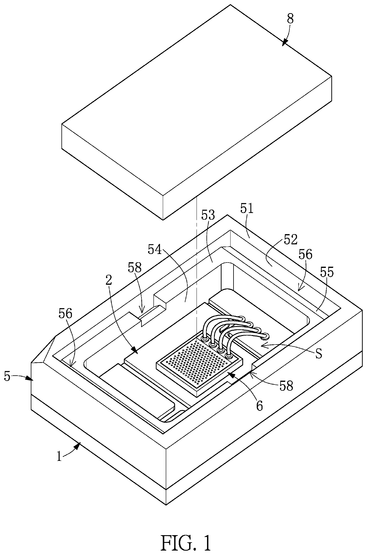
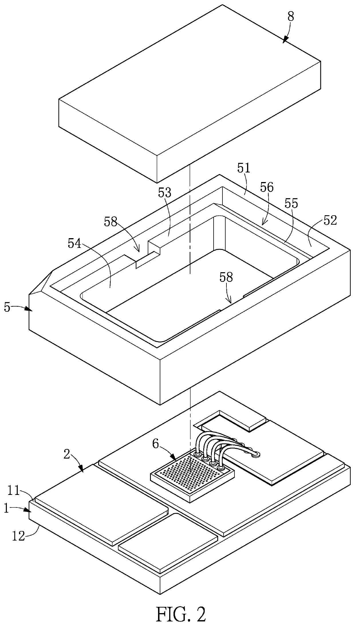
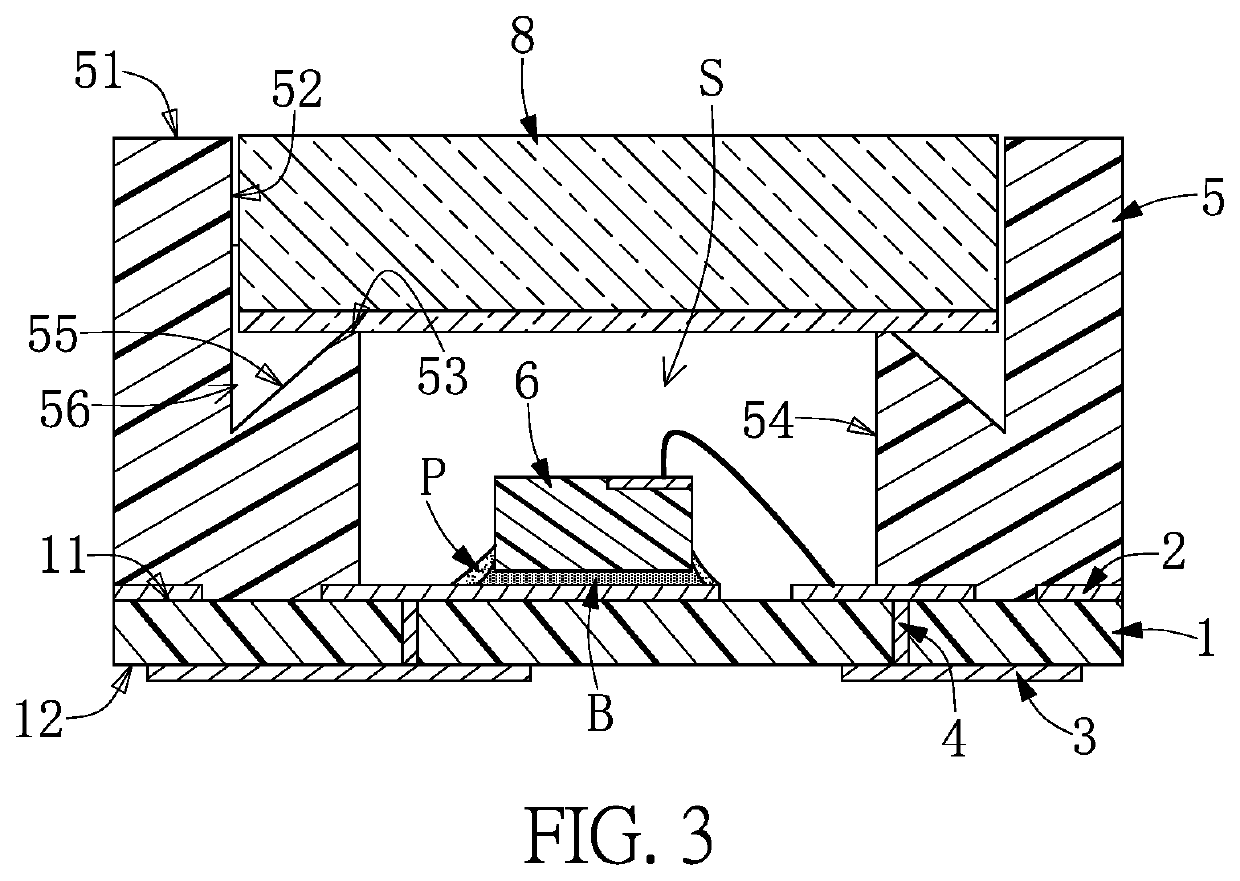
[0006]Therefore, the light source package structure of the present disclosure provides a structure that is different from a TO-CAN (Transistor Outline-CAN) package structure to meet different requirements nowadays. Specifically speaking, the fillers of the conductive adhesive are partially filled within the gap between the surrounding wall and the light permeable element. Accordingly, the conductive adhesive does not collapse from the gap, so that a bridge of the electrical connection can be improved through the fillers of the conductive adhesive.

Problems solved by technology

However, as there have been no major structural improvements in recent years, the conventional light source package structures have become increasingly difficult to meet various requirements.

Method used


Image

  • Light source package structure
  • Light source package structure
  • Light source package structure

Examples


Embodiment Construction

[0016]The present disclosure is more particularly described in the following examples that are intended as illustrative only since numerous modifications and variations therein will be apparent to those skilled in the art. Like numbers in the drawings indicate like components throughout the views. As used in the description herein and throughout the claims that follow, unless the context clearly dictates otherwise, the meaning of “a”, “an”, and “the” includes plural reference, and the meaning of “in” includes “in” and “on”. Titles or subtitles can be used herein for the convenience of a reader, which shall have no influence on the scope of the present disclosure.

[0017]The terms used herein generally have their ordinary meanings in the art. In the case of conflict, the present document, including any definitions given herein, will prevail. The same thing can be expressed in more than one way. Alternative language and synonyms can be used for any term(s) discussed herein, and no spec...


PUM

PropertyMeasurementUnit
particle diameteraaaaaaaaaa
mass fractionaaaaaaaaaa
angleaaaaaaaaaa

Abstract

A light source package structure is provided. The light source package structure includes a substrate, an upper electrode layer and a lower electrode layer respectively disposed on two sides of the substrate, a light emitting unit mounted on the upper electrode layer, a surrounding wall disposed on the substrate and arranged to surround the light emitting unit, a conductive unit disposed on the surrounding wall and electrically connected to the lower electrode layer, a light permeable element disposed on the surrounding wall, a detection circuit formed on the light permeable element, and at least one conductive adhesive. The conductive adhesive includes a colloid and a plurality of fillers mixed with the colloid. The colloid and the fillers of the conductive adhesive are partially filled within the gap.

Description

CROSS-REFERENCE TO RELATED PATENT APPLICATION[0001]This application claims the benefit of priority to China Patent Application No. 202010004957.9, filed on Jan. 3, 2020, and No. 201910378781.0, filed on May 7, 2019, in People's Republic of China. The entire content of the above identified application is incorporated herein by reference.[0002]Some references, which may include patents, patent applications and various publications, may be cited and discussed in the description of this disclosure. The citation and / or discussion of such references is provided merely to clarify the description of the present disclosure and is not an admission that any such reference is “prior art” to the disclosure described herein. All references cited and discussed in this specification are incorporated herein by reference in their entireties and to the same extent as if each reference was individually incorporated by reference.FIELD OF THE DISCLOSURE[0003]The present disclosure relates to a light sour...

Claims


Application Information

Patent Timeline
Patent Type & Authority Applications(United States)
IPC IPC(8): F21V23/00C09J9/02F21K9/00
CPCF21V23/002F21K9/00C09J9/02F21Y2115/30H01L33/486H01L33/62
Inventor LEE, WENHUNG, HSIANG-CHIHLYU, DA-PENGYANG, SHU-HUASU, YU-HUNG
Owner LITE ON OPTO TECH (CHANGZHOU) CO LTD
Learn More