
Semiconductor component, assembly and method for manufacturing semiconductor component

Active Publication Date: 2020-12-10
SHINDENGEN ELECTRIC MFG CO LTD
View PDF0 Cites 1 Cited by
  • Summary
  • Abstract
  • Description
  • Claims
  • Application Information

AI Technical Summary

Benefits of technology

The present invention provides a semiconductor component with a winding wire part in the semiconductor layer. This allows for a smaller and more efficient winding wire design that can detect changes in current accurately. The miniaturization of the winding wire part also allows for the creation of smaller semiconductor components. Additionally, this invention allows for the detection of existing semiconductor device operations and provides high versatility.

Problems solved by technology

However, conventional sensors cannot detect a change in current flowing through the semiconductor device with sufficient accuracy, and there is a problem that the size of the entire device including the sensor may be increased.

Method used


Image

  • Semiconductor component, assembly and method for manufacturing semiconductor component
  • Semiconductor component, assembly and method for manufacturing semiconductor component
  • Semiconductor component, assembly and method for manufacturing semiconductor component

Examples


first embodiment

>

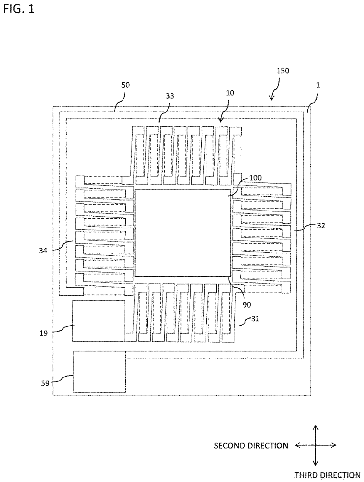
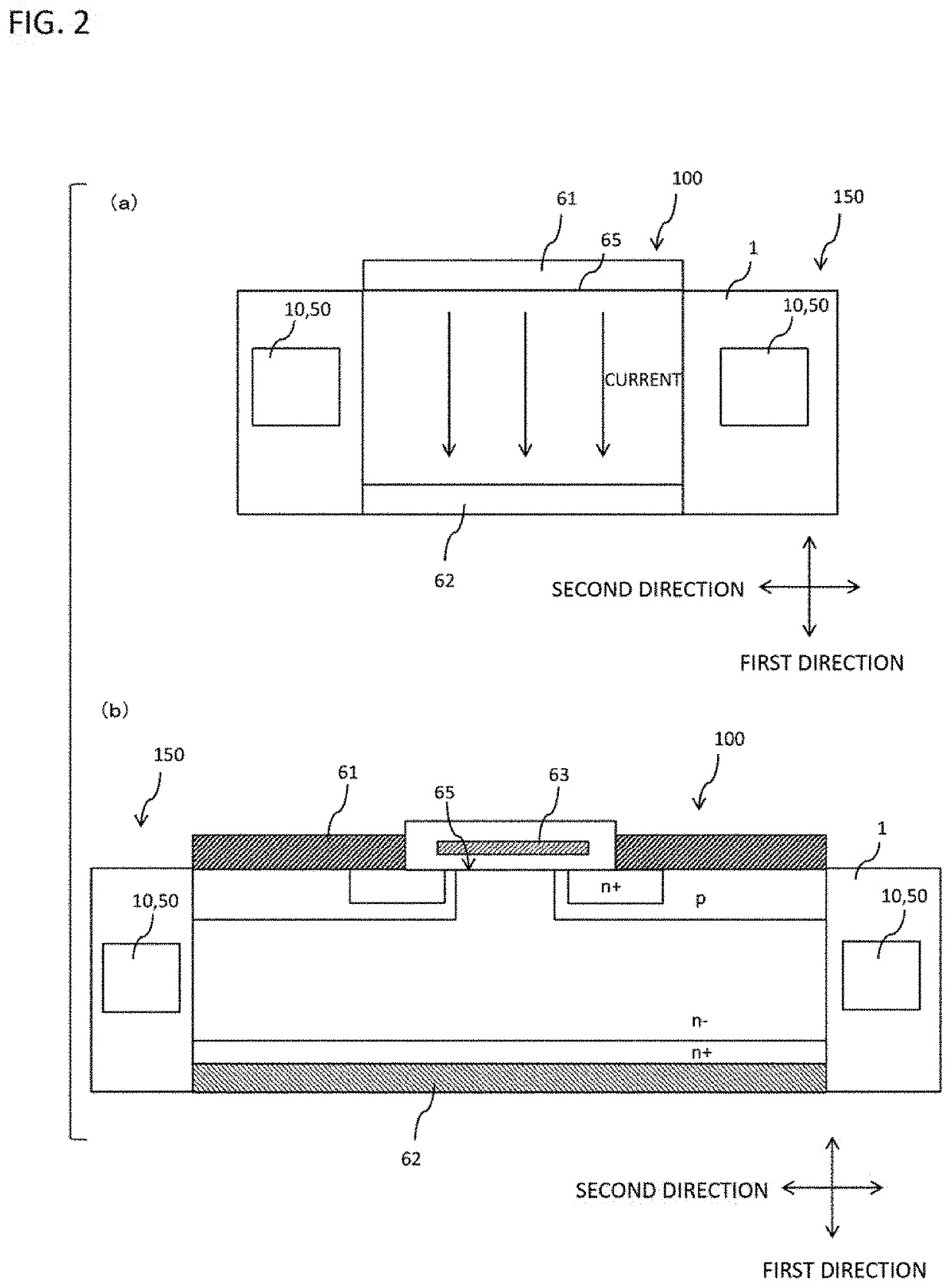
[0057]A semiconductor component, a combination, and a method of manufacturing the semiconductor component according to the present embodiment will be described. In the present embodiment, “one side” means the upper side in FIG. 2 and “other side” means the lower side in FIG. 2. Further, the vertical direction in FIG. 2 (the direction from the other side toward one side and the direction from one side toward the other side) is referred to as a “first direction”, the horizontal direction in FIG. 2 is referred to as a “second direction”, and the front-back direction of the page of FIG. 2 is referred to as a “third direction”. An in-plane direction including the second direction and the third direction is referred to as a “plane direction”, and a state where the view from the upper side in FIG. 2 is referred to as a “plan view”.

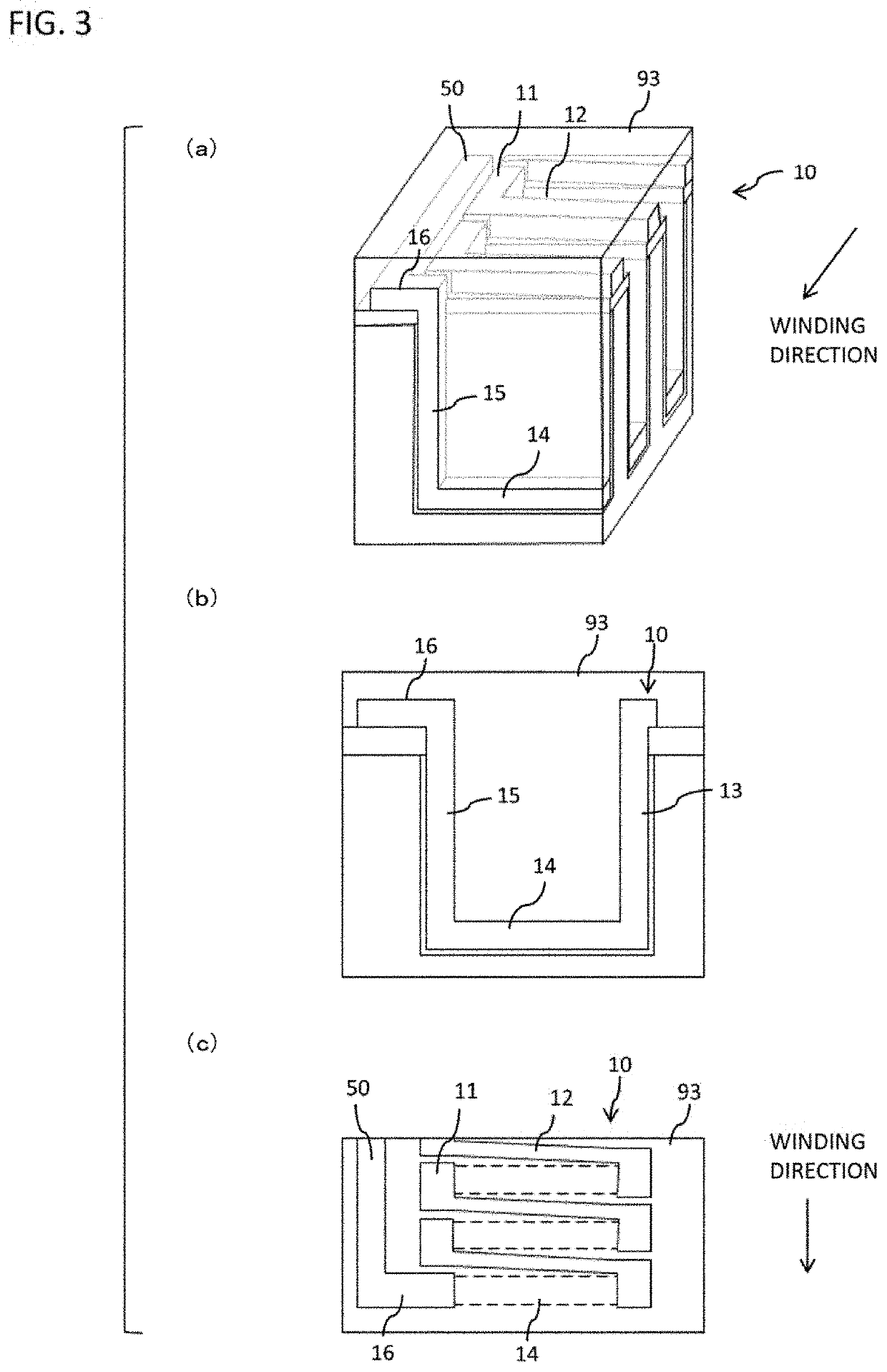
[0058]As shown in FIG. 1, a semiconductor component 150 of the present embodiment may have a semiconductor layer 1 including a winding wire part 10 and a windin...

second embodiment

[0095]Next, a second embodiment of the present invention will be described.

[0096]In the first embodiment, an aspect in which the winding return wire part 50 is provided outward of the periphery of the winding wire part 10 is used, but in the second embodiment, an aspect in which the winding return wire part 50 is provided inward of the periphery of the winding wire part 10 is used. Otherwise, any configuration used in the first embodiment can be used in the second embodiment. The members described in the first embodiment are described with the same reference numerals.

[0097]In the present embodiment, unlike the first embodiment, the semiconductor component may have the first straight part 11 along the winding direction, the second straight part 12 extending toward the peripherally outward (left side in FIG. 12) from the end of the first straight part 11 and extending in the plane direction toward the winding direction, the third straight part 13 extending from one side toward the oth...

third embodiment

[0101]Next, a third embodiment of the present invention will be described.

[0102]In the third embodiment, as shown in FIGS. 13 and 14, the semiconductor component 150 has a plurality of measurement units 170 (170a to 170d), and each measurement unit 170 has the winding wire part 10 and the winding return wire part 50. The terminal end part of the winding wire part 10 of one measurement unit 170 (for example, the first measurement unit 170a) is connected to the starting end part of the winding wire part10 of another measurement unit 170 (for example, the second measurement unit 170b), and the starting end part of the winding return wire part 50 of the one measurement unit 170 (for example, the first measurement unit 170a) is connected to the terminal end part of the winding return wire part 50 of the other measurement unit 170 (for example, the second measurement unit 170b). Otherwise, any configuration used in each of the above embodiments can be used in this embodiment. The members ...


PUM


Abstract

A semiconductor component 150 has a semiconductor layer 1 including a winding wire part 10 and a winding return wire part 50 connected at a terminal end part of the winding wire part 10 and returning from the terminal end part toward a starting end part side, wherein the semiconductor component is disposed so as to surround an object to be measured.

Description

TECHNICAL FIELD[0001]The present invention relates to a semiconductor component and an assembly having a winding wire part in a semiconductor layer, and a method for manufacturing a semiconductor component.BACKGROUND ART[0002]Conventionally, a current detection sensor using a Rogowski coil has been known. The Rogowski coil is a coreless coil, and has a winding core, a winding wire wound around the winding core, and a return wire connected to the terminal end part of the winding wire and returning to a starting end part side (for example, see JP 2012-88224 A). In addition, the Rogowski coil is connected to an integrator, and a change in current in an object to be measured can be measured by integrating the output voltage with the integrator. In such a Rogowski coil, the sensitivity is increased with an increase in the number of turns per unit distance.[0003]Meanwhile, a sensor has been proposed which detects a change in current flowing through a semiconductor device (for example, a s...

Claims


Application Information

Patent Timeline
IPC IPC(8): G01R19/00G01R15/18G01R15/12
CPCG01R15/12G01R19/0092G01R15/181G01R3/00
Inventor SUZUKI, KENICHISASHIDA, KAZUYUKIYAMAJI, MIZUEYOSHIDA, KENICHIKUNORI, SHINJI
Owner SHINDENGEN ELECTRIC MFG CO LTD
Learn More