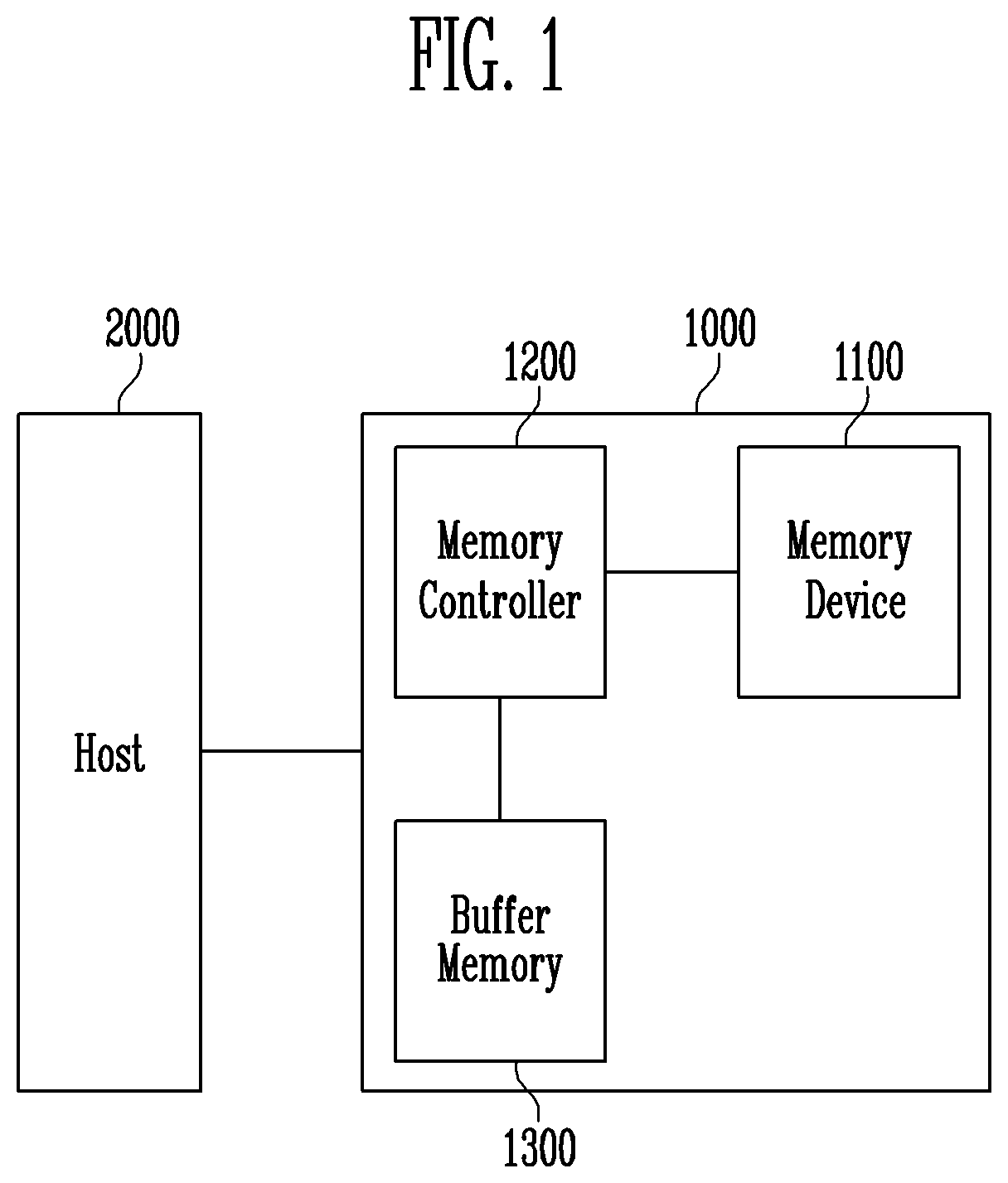
Memory device and operating method thereof
a memory device and operating method technology, applied in the field of memory devices and an operating method thereof, can solve problems such as data loss of volatile memory devices
- Summary
- Abstract
- Description
- Claims
- Application Information
AI Technical Summary
Benefits of technology
Problems solved by technology
Method used
Image


Examples
first embodiment
[0071]FIG. 6 is a diagram illustrating a bit line precharging method in a program verify operation according to the present disclosure.
[0072]Referring to FIG. 6, in the first embodiment, a program verify operation performed in a program operation using an MLC method is shown. During the program verify operation, bit lines may be selectively precharged according to a verify voltage corresponding to a read voltage. In FIG. 6, reference numeral 61 denotes a method of precharging bit lines during a read operation and reference numeral 62 denotes a method of selectively precharging bit lines during a program verify operation.
[0073]Since the method of precharging the bit lines as shown in 61 is the same as the method described with reference to FIG. 4, a detailed description thereof will be omitted.
[0074]Referring to reference numeral 62, the first to third verify voltages Vf1 to Vf3 used in the program verify operation may correspond to the first to third read voltages R1 to R3, respecti...
second embodiment
[0077]FIG. 7 is a diagram illustrating a bit line precharging method in a program verify operation according to the present disclosure.
[0078]Referring to FIG. 7, according to the second embodiment, in a memory device according to a TLC method where read operations are performed in a first order (read order), a bit line precharging method in a program verify operation is shown.
[0079]In the TLC method, three bits of data may be stored in a single memory cell. Memory cells may be programmed into one of the erase state ER and the first to seventh program states PV1 to PV7. The three bits of data may be defined as logical data corresponding to different logical pages. In other words, the three bits of data may consist of LSB data, CSB data and MSB data. For example, when the LSB, CSB and MSB data of the memory cells in the erase state ER are defined as 1, 1, and 1, respectively, a gray code of the erase state ER may be 111. When the LSB, CSB and MSB data of the memory cells in the first ...
third embodiment
[0110]FIG. 8 is a diagram illustrating a bit line precharging method in a program verify operation according to the present disclosure.
[0111]Referring to FIG. 8, according to the third embodiment, in a memory device according to a TLC method where read operations are performed in a second order (read order), a bit line precharging method in a program verify operation is shown. In FIG. 8, overlapping contents with FIG. 7 will be omitted.
[0112]In FIG. 8, the order of the read voltages shown on the right side of threshold voltages may refer to the order of read operations, and the drawing of Vf1 to Vf7 as shown below the threshold voltages illustrates a method of selectively precharging bit lines during a program verify operation. In FIG. 8, a program verify operation when read operations of reading logical data are performed in order from a low level to a high level is described as an example.
[0113]Referring to FIG. 8, read operations are described below.
[0114]In an LSB read operation...
PUM
 Abstract
Description
Claims
Application Information
 - R&D
- Intellectual Property
- Life Sciences
- Materials
- Tech Scout
- Unparalleled Data Quality
- Higher Quality Content
- 60% Fewer Hallucinations
Browse by: Latest US Patents, China's latest patents, Technical Efficacy Thesaurus, Application Domain, Technology Topic, Popular Technical Reports.
© 2025 PatSnap. All rights reserved.Legal|Privacy policy|Modern Slavery Act Transparency Statement|Sitemap|About US| Contact US: help@patsnap.com