Light-emitting element, and display, illuminator, and sensor each including same
a technology of light-emitting elements and sensors, which is applied in the direction of identification means, instruments, and organic compounds of group 3/13 elements, can solve the problems of color purity, light emission color purity, and the efficiency of delivery and receipt of singlets, and achieve high color purity and luminous efficiency.
- Summary
- Abstract
- Description
- Claims
- Application Information
AI Technical Summary
Benefits of technology
Problems solved by technology
Method used
Image


Examples
example 1
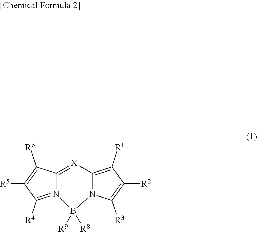
[0241]A glass substrate with an Ag0.98Pd0.01Cu0.01 alloy deposited thereon in a thickness of 100 nm and an ITO transparent electroconductive film deposited thereon in a thickness of 10 nm (manufactured by GEOMATEC Co., Ltd., 11 Ω / □, sputtered product) was cut into 38×46 mm, and etched. The resulting substrate was ultrasonically washed with “SEMICOCLEAN 56” (trade name, manufactured by Furuuchi Chemical Corporation) for 15 minutes, and then washed with ultrapure water. This substrate was treated with UV-ozone for 1 hour immediately before preparation of an element, and placed in a vacuum deposition apparatus. The air was evacuated until the degree of vacuum in the apparatus was 5×10⁻⁴ Pa or lower. By a resistance heating method, first, HAT-CN6 was deposited as a hole injection layer in a thickness of 10 nm, and HT-1 was deposited as a hole transporting layer in a thickness of 180 nm. Next, as an emissive layer, a host material H-1, a compound D-1 represented by general formula (1), a...
example 21
[0243]A glass substrate with an ITO transparent electroconductive film deposited thereon in a thickness of 165 nm (manufactured by GEOMATEC Co., Ltd., 11 Ω / □, sputtered product) was cut into 38×46 mm, and etched. The resulting substrate was ultrasonically washed with “SEMICOCLEAN 56” (trade name, manufactured by Furuuchi Chemical Corporation) for 15 minutes, and then washed with ultrapure water. This substrate was treated with UV-ozone for 1 hour immediately before preparation of an element, and placed in a vacuum deposition apparatus, and the air was evacuated until the degree of vacuum in the apparatus was 5×10⁻⁴ Pa or lower. By a resistance heating method, first, HAT-CN6 was deposited as a hole injection layer in a thickness of 10 nm, and HT-1 was deposited as a hole transporting layer in a thickness of 180 nm. Next, as an emissive layer, a host material H-1, a compound D-3 represented by general formula (1), and a compound B-1 represented by general formula (2) were deposited in...
examples 22 to 35
[0253]In the same manner as in Example 1 except that compounds described in Table 4 were used as materials for electron transporting layers, light-emitting elements were prepared and evaluated. The results are shown in Table 4. ET-2 to ET-8 are compounds shown below.
TABLE 4Emissive Layer*Numbers in parentheses belowcompound names: weight ratiosGeneralElectron transporting layerExternalformula (1)GeneralElectronquantumor otherformulaEmittedtransportingDonorefficiencyHostdopants(2)colormaterialmaterial(%)Example 22H-1D-1B-1RedET-22E-15.2(80)(1)(20)Example 23H-1D-1B-1RedET-32E-15.1(80)(1)(20)Example 24H-1D-3B-2GreenET-22E-14.8(80)(1)(20)Example 25H-1D-3B-2GreenET-32E-14.6(80)(1)(20)Example 26H-1D-1B-1RedET-42E-15.2(80)(1)(20)Example 27H-1D-1B-1RedET-52E-15.1(80)(1)(20)Example 28H-1D-3B-2GreenET-42E-14.7(80)(1)(20)Example 29H-2D-3B-2GreenET-52E-14.5(80)(1)(20)Example 30H-1D-1B-1RedET-62E-15.2(80)(1)(20)Example 31H-1D-1B-1RedET-72E-15.1(80)(1)(20)Example 32H-1D-1B-1RedET-82E-15.1(80)(1)(...
PUM
| Property | Measurement | Unit |
|---|---|---|
| wavelength range | aaaaa | aaaaa |
| wavelength range | aaaaa | aaaaa |
| width | aaaaa | aaaaa |
Abstract
Description
Claims
Application Information
 - R&D Engineer
- R&D Manager
- IP Professional
- Industry Leading Data Capabilities
- Powerful AI technology
- Patent DNA Extraction
Browse by: Latest US Patents, China's latest patents, Technical Efficacy Thesaurus, Application Domain, Technology Topic.
© 2024 PatSnap. All rights reserved.Legal|Privacy policy|Modern Slavery Act Transparency Statement|Sitemap