Method of patterning quantum dots, device using same, and system thereof

Active Publication Date: 2021-09-30
TCL CHINA STAR OPTOELECTRONICS TECH CO LTD
View PDF0 Cites 0 Cited by
  • Summary
  • Abstract
  • Description
  • Claims
  • Application Information

AI Technical Summary

Benefits of technology

[0027]Embodiments of the present application provide a method of patterning quantum dots, a device using same, and a system thereof. By powering the upper electrodes and the lower electrodes to form an electric field between the upper electrodes and the lower electrodes, quantum dot solution is gathered between the upper electrodes and the lower electrodes according to an electric field distribution. Subsequently, the quantum dot solution is deposited into a film by evaporation of a solvent, and a patterned quantum dot thin film is obtained on the base. The embodiments of the present application do not require special treatment on the base, such as processing patterned electrodes on the base, a patterned quantum dot thin film can be obtained, and requirement of a formulation system of the quantum dot solution is low. The method is

Problems solved by technology

Among them, heating, ultraviolet curing, and washing developer in the photolithography process will affect stability of the quantum dots, while ink requirements of the inkjet printing process are too high and without mature and

Method used


Image

  • Method of patterning quantum dots, device using same, and system thereof
  • Method of patterning quantum dots, device using same, and system thereof
  • Method of patterning quantum dots, device using same, and system thereof

Examples


Example

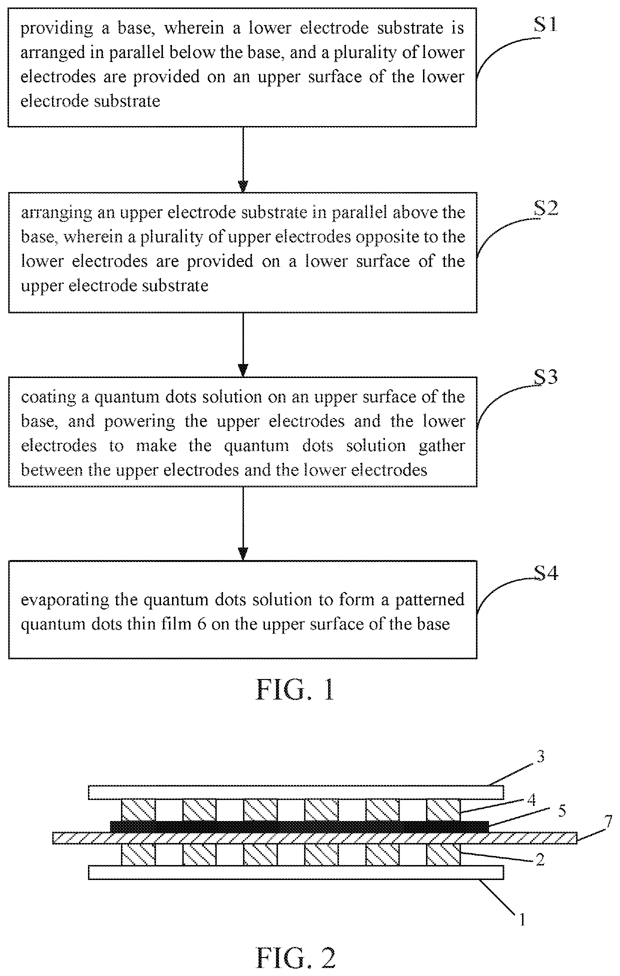
[0039]In order to illustrate the technical solutions of the present application or the related art in a clearer manner, the drawings desired for the present application or the related art will be described hereinafter briefly. Obviously, the following drawings merely relate to some embodiments of the present application, and based on these drawings, a person skilled in the art may obtain the other drawings without any creative effort.

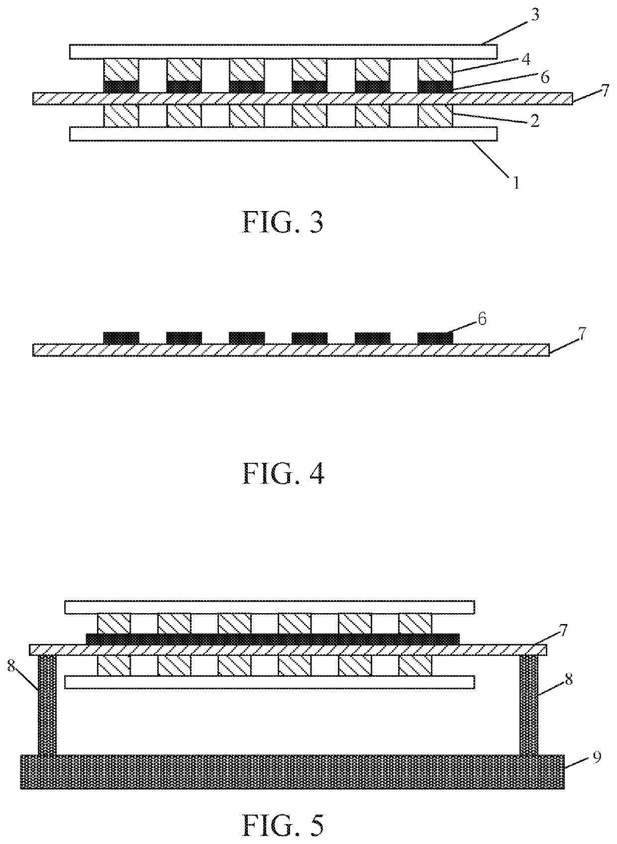
[0040]FIG. 1 is a schematic flowchart of a method of patterning quantum dots according to an embodiment of the present application, FIG. 2 is a schematic structural diagram of a device of patterning quantum dots according to an embodiment of the present application, and FIG. 3 is a schematic process diagram of the method of patterning quantum dots according to an embodiment of the present application. Combining FIG. 1, FIG. 2, and FIG. 3, the method includes steps as follows.

[0041]S1, providing a base 7, wherein a lower electrode substrate 1 is arranged...


PUM

PropertyMeasurementUnit
Thicknessaaaaaaaaaa
Diameteraaaaaaaaaa
Distributionaaaaaaaaaa

Abstract

A method of patterning quantum dots, a device using same, and a system thereof are provided. By providing a base between a plurality of upper electrodes and a plurality of lower electrodes, coating a quantum dot solution on an upper surface of the base, and powering the upper electrodes and the lower electrodes to form an electric field between the upper electrodes and the lower electrodes, the quantum dot solution is gathered between the upper electrodes and the lower electrodes according to an electric field distribution. Subsequently, the quantum dot solution can be deposited into a film by evaporation of a solvent, thereby obtaining a patterned quantum dot thin film on the base.

Description

FIELD OF INVENTION[0001]Embodiments of the present application relate to a technical field of quantum dots, and in particular, to a method of patterning quantum dots, a device using same, and a system thereof.BACKGROUND OF INVENTION[0002]Size of structural units of nanomaterials ranges from 1 nanometer to 100 nanometers, which is close to a coherence length of electrons, and nanomaterial properties are greatly changed due to self-organization brought by strong coherence. Moreover, scale of the nanomaterials is close to a wavelength of light, and they possess volume effect, surface effect, quantum size effect, and macroscopic quantum tunneling effect. Therefore, they have unique properties in melting point, magnetism, optics, thermal conductivity, electrical conductivity, etc., making them have important application value in many fields.[0003]Quantum dots (QDs) are a typical type of nanomaterials, which have characteristics of small size and high energy conversion efficiency. They ha...

Claims


Application Information

Patent Timeline
IPC IPC(8): C23C14/04H01L51/50H01L51/56C09K11/88C09K11/74H01L51/00
CPCC23C14/04H01L51/502H01L51/56B82Y20/00C09K11/7492H01L51/0014C09K11/883B82Y40/00H10K71/12H10K50/115B82Y10/00B82Y30/00H10K71/00H10K71/20
Inventor ZHAO, JINYANG
Owner TCL CHINA STAR OPTOELECTRONICS TECH CO LTD
Why Eureka
Try Eureka