Process proximity correction method and the computing device for the same

Pending Publication Date: 2022-02-03
SAMSUNG ELECTRONICS CO LTD
View PDF0 Cites 0 Cited by
  • Summary
  • Abstract
  • Description
  • Claims
  • Application Information

AI Technical Summary

Benefits of technology

The present invention provides a process proximity correction method and a process proximity correction computing device that can improve the accuracy of a target layout. This is achieved by converting a target layout including a plurality of patterns into an image, and then using machine learning to predict an after-cleaning image (ACI) based on the input of multiple zoomed out versions of the image. The predicted after-cleaning image is then compared with a target value to generate an after-cleaning image error, which is then used to adjust the target layout. This process can improve the accuracy of the target layout and enhance the overall quality of the final product.

Problems solved by technology

In the process of etching, process errors may occur due to various factors.
The factors that induce the process errors may be due to the characteristics of the process, but may also be due to characteristics of the pattern of the photoresist or the semiconductor pattern implemented by etching.

Method used


Image

  • Process proximity correction method and the computing device for the same
  • Process proximity correction method and the computing device for the same
  • Process proximity correction method and the computing device for the same

Examples


Embodiment Construction

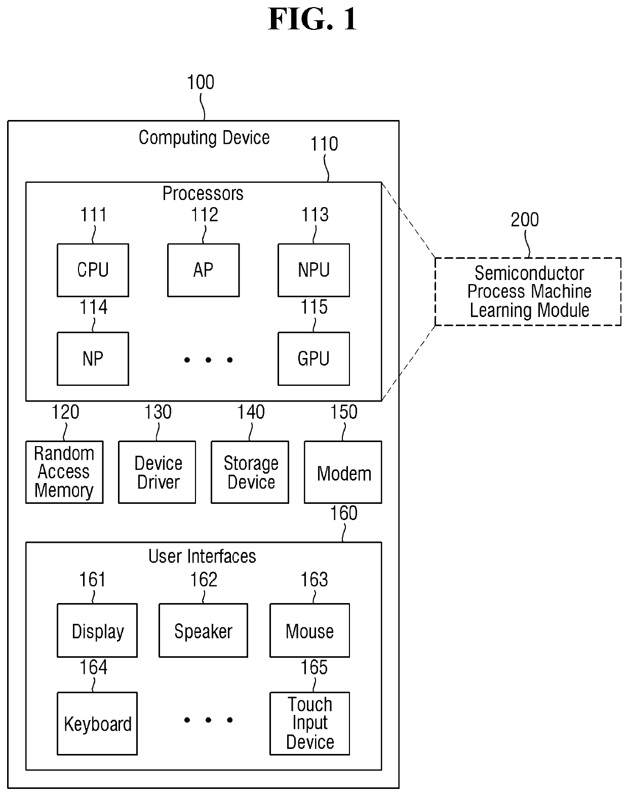
[0019]FIG. 1 is an exemplary block diagram showing a process proximity correction computing device according to some embodiments.

[0020]Referring to FIG. 1, a computing device 100 according to some embodiments may include a plurality of processors 110, a random access memory 120, a device driver 130, a storage device 140, a modem 150, and user interfaces 160.

[0021]At least one of the processors 110 may execute a semiconductor process machine learning module 200. The semiconductor process machine learning module 200 may generate a layout for fabricating a semiconductor device on the basis of machine learning. For example, the semiconductor process machine learning module 200 may be implemented in the form of commands (or codes) executed by at least one of the processors 110 (also described as software or computer program code executed by hardware). At this time, at least one processor may load the commands (or codes) of the semiconductor process machine learning module 200 into the ra...


PUM


Abstract

A process proximity correction method is performed by a process proximity correction computing device which performs a process proximity correction (PPC) through at least one of a plurality of processors. The process proximity correction method includes: converting a target layout including a plurality of patterns into an image, zooming-in or zooming-out the image at a plurality of magnifications to generate a plurality of input channels, receiving the plurality of input channels and performing machine learning to predict an after-cleaning image (ACI), comparing the predicted after-cleaning image with a target value to generate an after-cleaning image error, and adjusting the target layout on the basis of the after-cleaning image error.

Description

[0001]This application claims priority under 35 U.S.C. § 119 to Korean Patent Application No. 10-2020-0094254, filed on Jul. 29, 2020, the disclosure of which is incorporated herein by reference in its entirety.BACKGROUND1. Technical Field[0002]The present disclosure relates to a process proximity correction method and a computing device.2. Description of the Related Art[0003]A semiconductor process for fabricating semiconductor devices is implemented by a combination of various procedures such as etching, depositing, planarization, growth, and implantation. Etching may be performed by forming a photoresist pattern on a target and removing portions of the target not covered by photoresist through chemicals, gas, plasma, ion beams, or the like.[0004]In the process of etching, process errors may occur due to various factors. The factors that induce the process errors may be due to the characteristics of the process, but may also be due to characteristics of the pattern of the photores...

Claims


Application Information

Patent Timeline
IPC IPC(8): G03F1/36G03F1/76G06T7/00G06T3/40
CPCG03F1/36G03F1/76G06T2207/30148G06T3/4046G06T2207/20084G06T7/0006H01L21/0273H01L22/12H01L21/76816G06T3/40G06N20/00G06N3/08G06F30/3323G06F30/392
Inventor LEE, SOO YONGKANG, MIN-CHEOLKIM, U SEONGYANG, SEUNG HUNELEE, JEE YONG
Owner SAMSUNG ELECTRONICS CO LTD
Why Eureka
Try Eureka