Electro-optical device and electronic apparatus
- Summary
- Abstract
- Description
- Claims
- Application Information
AI Technical Summary
Benefits of technology
Problems solved by technology
Method used
Image

Examples
exemplary embodiment 1
[0029]1. Configuration of Electro-Optical Device 100
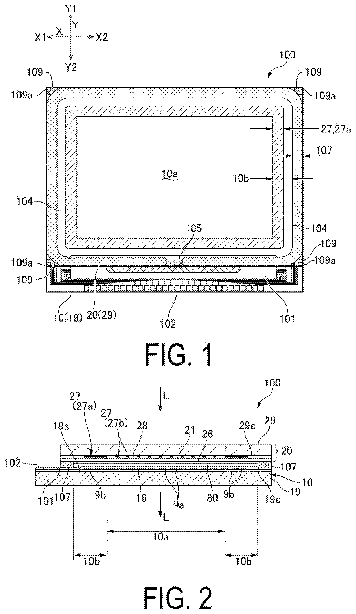
[0030]FIG. 1 is a plan view of an electro-optical device 100 according to Exemplary Embodiment 1 of the present disclosure. FIG. 2 is a cross-sectional view illustrating the electro-optical device 100 illustrated in FIG. 1. As illustrated in FIG. 1 and FIG. 2, in the electro-optical device 100, the first substrate 10 and the second substrate 20 are bonded together with a seal material 107 creating a predetermined gap, where the first substrate 10 is opposed to the second substrate 20. The seal material 107 is provided in a frame-like shape in conformance with the outer edge of the second substrate 20. An electro-optical layer 80 such as a liquid crystal layer is provided in an area surrounded by the seal material 107 between the first substrate 10 and the second substrate 20. The seal material 107 is a photocurable adhesive, or a photocurable and thermosetting adhesive, and a gap material such as glass fiber or glass beads for sett...
exemplary embodiment 2
[0084]FIG. 12 is an explanatory diagram of the electro-optical device 100 according to Exemplary Embodiment 2 of the present disclosure, and corresponds to FIG. 11 of Exemplary Embodiment 1. FIG. 12 schematically illustrates an enlarged periphery of the semiconductor layer 31a. FIG. 13 is a cross-sectional view of the electro-optical device 100 according to Exemplary Embodiment 2 of the present disclosure, and corresponds to FIG. 5 of Exemplary Embodiment 1. FIG. 13 schematically illustrates a state in which the electro-optical device 100 is cut corresponding to an A1-A1′ line illustrated in FIG. 4. Note that the basic configuration of this exemplary embodiment and exemplary embodiments to be described later is the same as the configuration of Exemplary Embodiment 1, and thus common portions have the same reference symbols and a description of the common portions will be omitted.
[0085]As illustrated in FIG. 12 and FIG. 13, in the present exemplary embodiment as well, the first light...
exemplary embodiment 3
[0089]FIG. 14 is an explanatory diagram of the electro-optical device 100 according to Exemplary Embodiment 3 of the present disclosure, and corresponds to FIG. 11 of Exemplary Embodiment 1. FIG. 14 schematically illustrates an enlarged periphery of the semiconductor layer 31a. FIG. 15 is a cross-sectional view of the electro-optical device 100 according to Exemplary Embodiment 3 of the present disclosure. FIG. 15 schematically illustrates a state in which the electro-optical device 100 is cut corresponding to the A1-A1′ line illustrated in FIG. 4.
[0090]As illustrated in FIG. 12 and FIG. 13, in the present exemplary embodiment as well, the first light shielding wall 8a1 and the second light shielding wall 8a2 are provided on sides of the semiconductor layer 31a respectively in the same manner as in Exemplary Embodiment 1. In the present exemplary embodiment, the width Wa of the first contact region 31e of the semiconductor layer 31a to which the first capacitance electrode 4a is ele...
PUM
 Abstract
Description
Claims
Application Information
 - R&D Engineer
- R&D Manager
- IP Professional
- Industry Leading Data Capabilities
- Powerful AI technology
- Patent DNA Extraction
Browse by: Latest US Patents, China's latest patents, Technical Efficacy Thesaurus, Application Domain, Technology Topic.
© 2024 PatSnap. All rights reserved.Legal|Privacy policy|Modern Slavery Act Transparency Statement|Sitemap