Identifying test coverage gaps for integrated circuit designs based on node testability and physical design data

a technology of integrated circuit design and test coverage, applied in computer aided design, instruments, measurement devices, etc., can solve the problems of not being able to achieve 100% test coverage, unable to design a chip without any mistakes, and unable to manufacture a chip without any defects,

Pending Publication Date: 2022-04-28
NXP USA INC
View PDF0 Cites 2 Cited by
  • Summary
  • Abstract
  • Description
  • Claims
  • Application Information

AI Technical Summary

Problems solved by technology

The design and fabrication of electronic systems, such as very large scale (VLSI) integrated circuits (ICs), is a very complex and thorough process.
The design size and complexity of today's chips/circuits make it nearly impossible to design a chip without any mistakes or manufacture a chip without any defects.
However, obtaining 100% test coverage is generally not feasible or possible with today's IC designs because they have become increasingly complex with greater levels of circuit density.
Although conventional test coverage analysis tools are able to determine whether a given test is achieving test coverage goals, they are generally not qualitative enough to meet defectivity coverage goals of critical safety-related application spaces such as automotive, medical and aerospace where the test quality requirements are very high,

Method used


Image

  • Identifying test coverage gaps for integrated circuit designs based on node testability and physical design data
  • Identifying test coverage gaps for integrated circuit designs based on node testability and physical design data
  • Identifying test coverage gaps for integrated circuit designs based on node testability and physical design data

Examples


Embodiment Construction

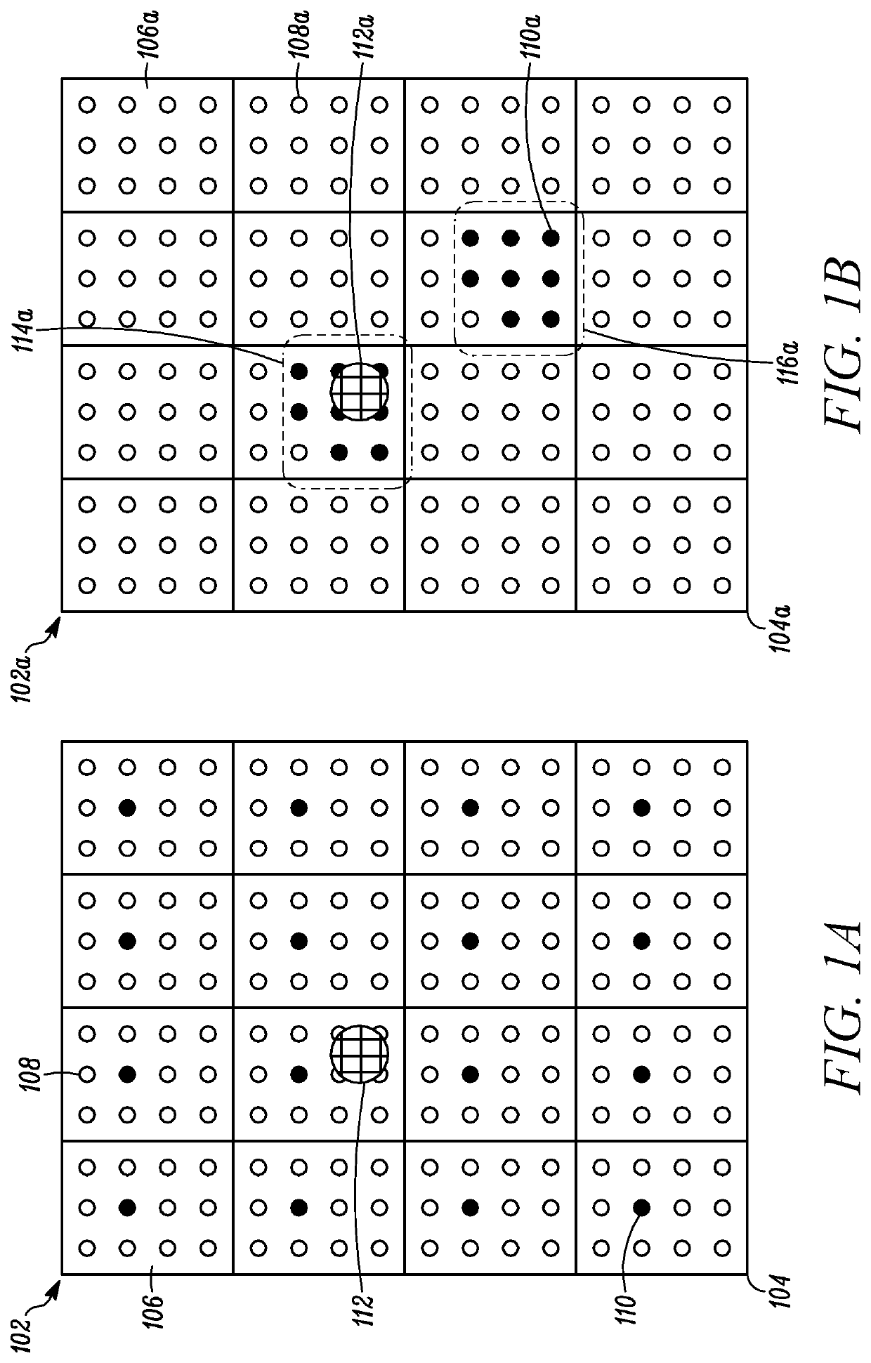
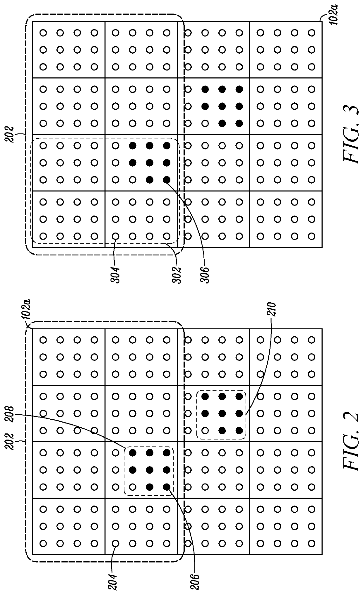
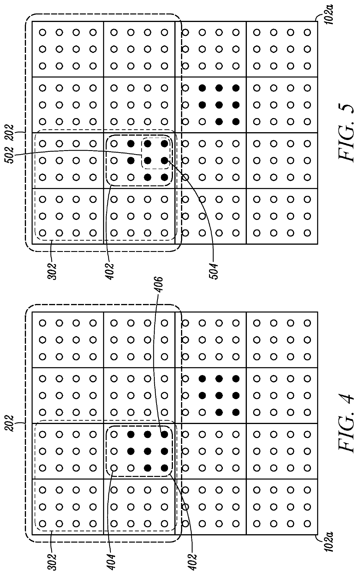
[0028]Conventional test coverage analysis tools generally provide an abstract test coverage metric that is based on the number of testable and untestable nodes. For example, consider a scenario where a design / chip comprises 1,000,000 total testable nodes which are connectors of logical cells. The total number of testable nodes can be defined as a total number of nodes in the design (or area of interest) minus a total number of untestable nodes in the design (or area of interest). Nodes can be untestable for various reasons such as, but not limited to, architectural limitations. In this example, 920,000 of the nodes have been tested, and 80,000 of the nodes have not been tested. A conventional test coverage analysis tool would typically utilize only these tested / untested node counts at a modular level to determine that, in this example, the test under analysis has 92% test coverage. The resulting percentage, Pcov, is a representation of a probability of a test program screening a def...


PUM


Abstract

Test coverage for a circuit design may be determined by obtaining node testability data and physical location data for each node of a plurality of nodes in the circuit design. A determination is made that one or more low test coverage areas within the circuit design include untested nodes based on the node testability data and the physical location data of each node of the plurality of nodes. Test coverage data is generated for the circuit design including at least an identification of the one or more low test coverage areas.

Description

BACKGROUNDField[0001]The present invention generally relates to the field of electronic circuit design and, more particularly, relates to determining low-test coverage areas for integrated circuit designs.Related Art[0002]The design and fabrication of electronic systems, such as very large scale (VLSI) integrated circuits (ICs), is a very complex and thorough process. The design size and complexity of today's chips / circuits make it nearly impossible to design a chip without any mistakes or manufacture a chip without any defects. Therefore, IC designers implement various testing tools and methodologies to help ensure that a logical design of a chip conforms to its functional specification and that manufacturing defects are identifiable after the chip has been fabricated. Examples of these testing tools and methodologies include functional verification and Design for Testability (DFT) techniques. Functional verification tools can be used to confirm the functionality and logical behavi...

Claims


Application Information

Patent Timeline
IPC IPC(8): G06F30/398G06F30/392
CPCG06F30/398G06F30/392G06F30/394G06F30/396G01R31/31835
Inventor JINDAL, ANURAGNARULA, KAPILKALYAN, RAHULLIANG, HONGKUN
Owner NXP USA INC
Why Eureka
Try Eureka