Semiconductor device including conductive line and method for manufacturing the same
- Summary
- Abstract
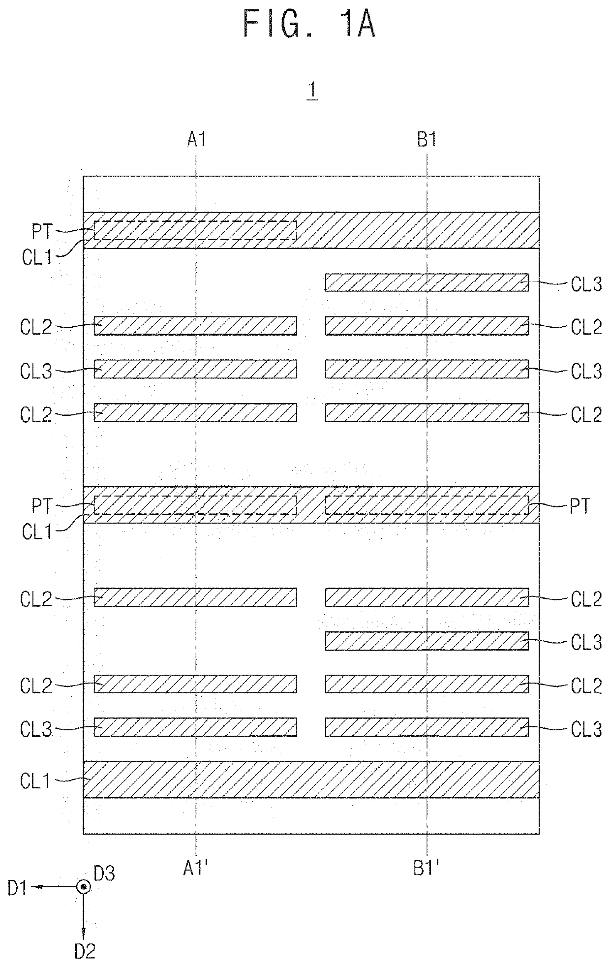
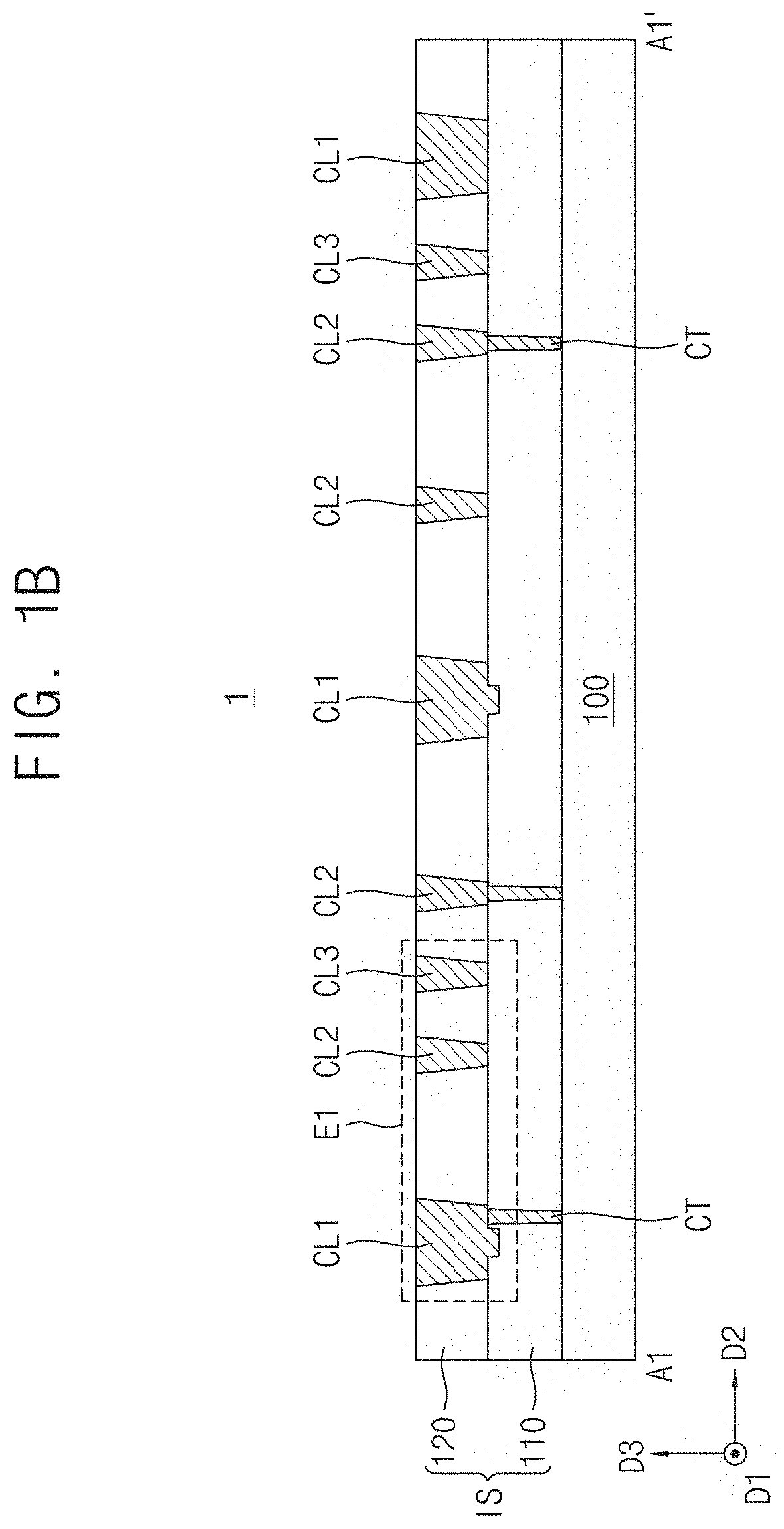
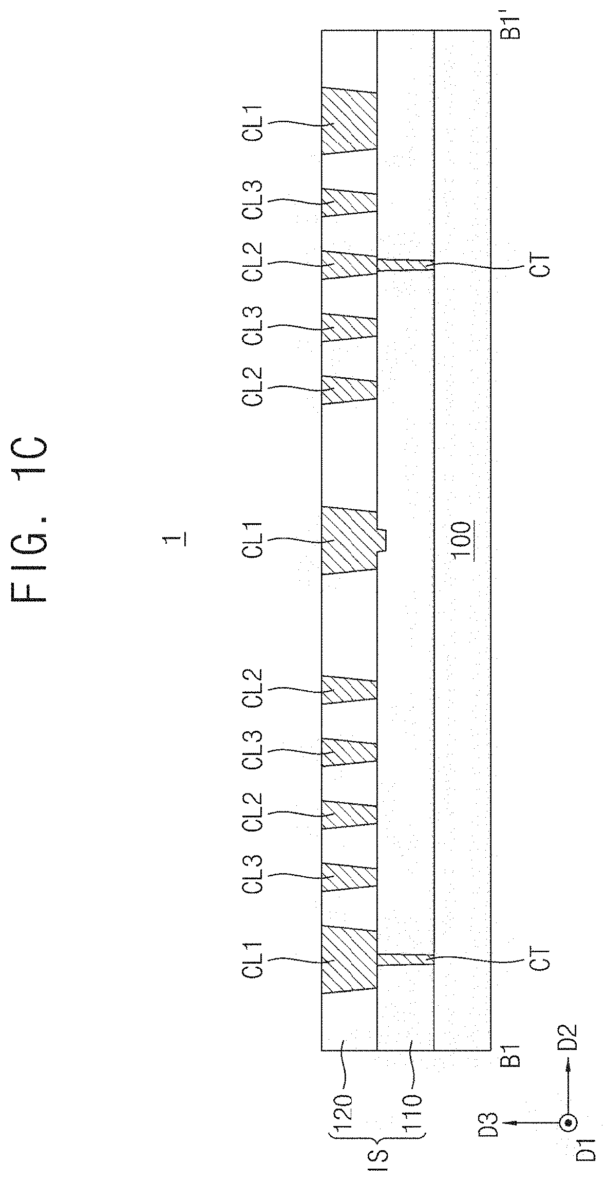
- Description
- Claims
- Application Information
AI Technical Summary
Benefits of technology
Problems solved by technology
Method used
Image

Examples
Example
[0032]While the term “same,”“equal” or “identical” is used in description of example embodiments, it should be understood that some imprecisions may exist. Thus, when one element is referred to as being the same as another element, it should be understood that an element or a value is the same as another element within a desired manufacturing or operational tolerance range (e.g., ±10%).
[0033]When the terms “about” or “substantially” are used in this specification in connection with a numerical value, it is intended that the associated numerical value includes a manufacturing or operational tolerance (e.g., ±10%) around the stated numerical value. Moreover, when the words “about” and “substantially” are used in connection with geometric shapes, it is intended that precision of the geometric shape is not required but that latitude for the shape is within the scope of the disclosure. Further, regardless of whether numerical values or shapes are modified as “about” or “substantially,” i...
PUM
 Abstract
Description
Claims
Application Information
 - R&D Engineer
- R&D Manager
- IP Professional
- Industry Leading Data Capabilities
- Powerful AI technology
- Patent DNA Extraction
Browse by: Latest US Patents, China's latest patents, Technical Efficacy Thesaurus, Application Domain, Technology Topic.
© 2024 PatSnap. All rights reserved.Legal|Privacy policy|Modern Slavery Act Transparency Statement|Sitemap