Die coat perimeter to enhance semiconductor reliability

Inactive Publication Date: 2008-08-21
ANALOG DEVICES INC
View PDF4 Cites 17 Cited by
  • Summary
  • Abstract
  • Description
  • Claims
  • Application Information

AI Technical Summary

Benefits of technology

[0013]The present invention, therefore, provides a method to enhance reliability of a semiconductor package, wherein the method comprises: (a) constructing a peripheral wall on the semiconductor die, said peripheral wall isolating a stress sensitive area from remaining area of the semiconductor die; and (b) depositing die coat material on the remaining area of the semiconductor die wherein the peripheral wall constrains the flow of the die coat material in the stress sensitive area of said semiconductor die. The peripheral wall, by constraining flow of the die coat material, prevents stress on the bond wires caused by mismatch in coefficient of thermal expansion between the die coat and the semiconductor die.
[0014]In another embodiment, the present invention provides for a method to enhance reliability of a semiconductor package, wherein the method comprises: (a) constructing a polymer dam on the semiconductor die wherein the polymer dam isolates a stress sensitive area from the remaining area of the semiconductor die; and (b) depositing die coat material on the remaining area of the semiconductor die such that the polymer dam constraining flow of the die coat material in said stress sensitive area of said semiconductor die. The peripheral wall, by constraining flow of said die material, prevents stress on the bond wires caused by mismatch in coefficient of thermal expansion between the die coat and the semiconductor die.
[0015]The present invention, in one embodiment, provides for a semiconductor package having enhanced reliability comprising: (a) a semiconductor die; (b) a peripheral wall formed

Problems solved by technology

The performance of many semiconductor devices can be negatively impacted by the plastic packaging process.
This contact can cause a fluctuation in the performance and reliability of the product due to thermal coefficient of expansion mismatches between the silicon semiconductor device and the plastic package molding compound.
Unfortunately, silicone die coats when in contact with package bond wires stress those bond wires during thermal cycles due to mismatched coefficient of thermal expansions (CTEs).
Specifically, in high-performance semiconductor packaging structures, a temperature coefficient mismatch occurs due to the uneven expansion of the plastic molding compound as co

Method used


Image

  • Die coat perimeter to enhance semiconductor reliability
  • Die coat perimeter to enhance semiconductor reliability
  • Die coat perimeter to enhance semiconductor reliability

Examples


Example

[0026]While this invention is illustrated and described in a preferred embodiment, the invention may be produced in many different configurations. There is depicted in the drawings, and will herein be described in detail, a preferred embodiment of the invention, with the understanding that the present disclosure is to be considered as an exemplification of the principles of the invention and the associated functional specifications for its construction and is not intended to limit the invention to the embodiment illustrated. Those skilled in the art will envision many other possible variations within the scope of the present invention.

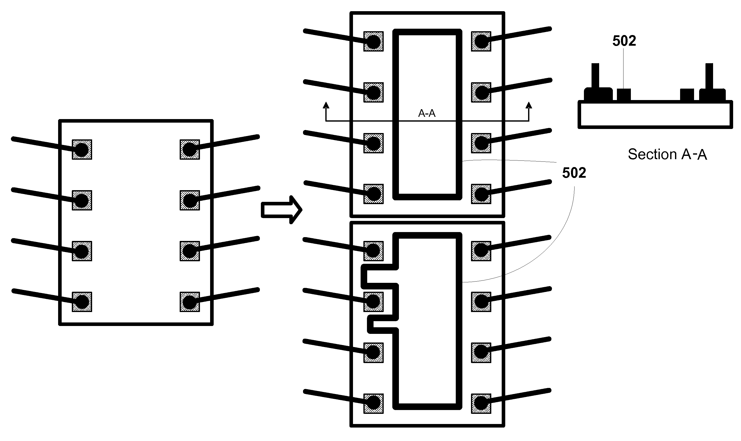
[0027]The present invention provides for a method of creating die coat perimeter (such as a dam) to enhance semiconductor reliability. The present invention's construction of a peripheral wall (dam) which constrains the flow of die surface stress relieving die coating materials such as silicone gels or other stress relieving materials to ensure it does...


PUM


Abstract

A semiconductor packaging stress relief technique with enhanced reliability. Reliability is enhanced over conventional post wirebond assembly die coating processes by forming a peripheral wall on the semiconductor die isolating the stress sensitive area from remaining area in the semiconductor die, and depositing die coat material constraining the flow of the die coat material in the stress sensitive area of the semiconductor die. The peripheral wall, by constraining flow of the die coat material, prevents stress on the package bond wires caused by mismatch in coefficient of thermal expansion between the die coat and the package bond wires which are encased in the plastic molding compound.

Description

BACKGROUND OF THE INVENTION[0001]1. Field of Invention[0002]The present invention relates generally to the field of semiconductor packaging. More specifically, the present invention is related to a method for enhancing the reliability of stress relief coatings commonly used in plastic semiconductor packaging.[0003]2. Discussion of Prior Art[0004]The performance of many semiconductor devices can be negatively impacted by the plastic packaging process. The typical plastic packaging process results in direct physical contact of the semiconductor device with the plastic mold compound. This contact can cause a fluctuation in the performance and reliability of the product due to thermal coefficient of expansion mismatches between the silicon semiconductor device and the plastic package molding compound. Silicone die coats are excellent stress relief materials for use in semiconductor packages. Unfortunately, silicone die coats when in contact with package bond wires stress those bond wire...

Claims


Application Information

Patent Timeline
IPC IPC(8): H01L23/29H01L21/00H01L23/24
CPCH01L23/296H01L23/3114H01L2924/10253H01L2224/32245H01L24/49H01L24/48H01L2924/14H01L2924/12044H01L2924/01013H01L2224/73265H01L2224/49171H01L2224/48465H01L2224/48247H01L23/3135H01L2924/00012H01L2924/00H01L2924/181H01L2224/05554H01L2224/8592H01L2924/00014H01L2924/10161H01L2224/45099H01L2224/45015H01L2924/207
Inventor GOIDA, THOMAS
Owner ANALOG DEVICES INC
Why Eureka
Try Eureka