[0042]Hereinafter, exemplary embodiments of the present invention will be described in detail with reference to the accompanying drawing figures.
[0043]In the following description, same drawing reference numerals are used for the same elements even in different drawings. The matters defined in the description such as a detailed construction and elements are nothing but the ones provided to assist in a comprehensive understanding of the invention. Thus, it is apparent that the present invention can be carried out without those defined matters. Also, well-known functions or constructions are not described in detail since they would obscure the invention in unnecessary detail.
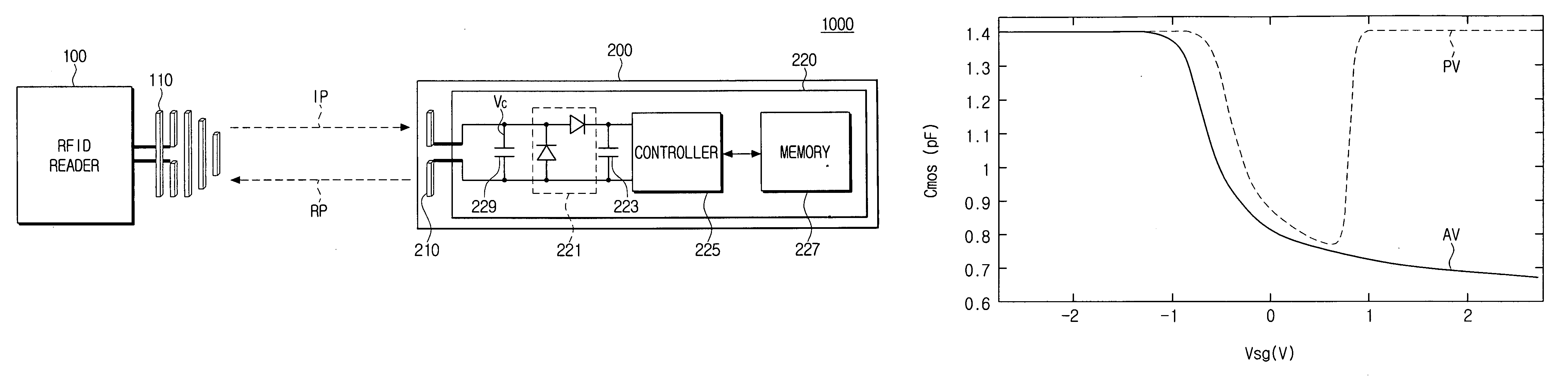
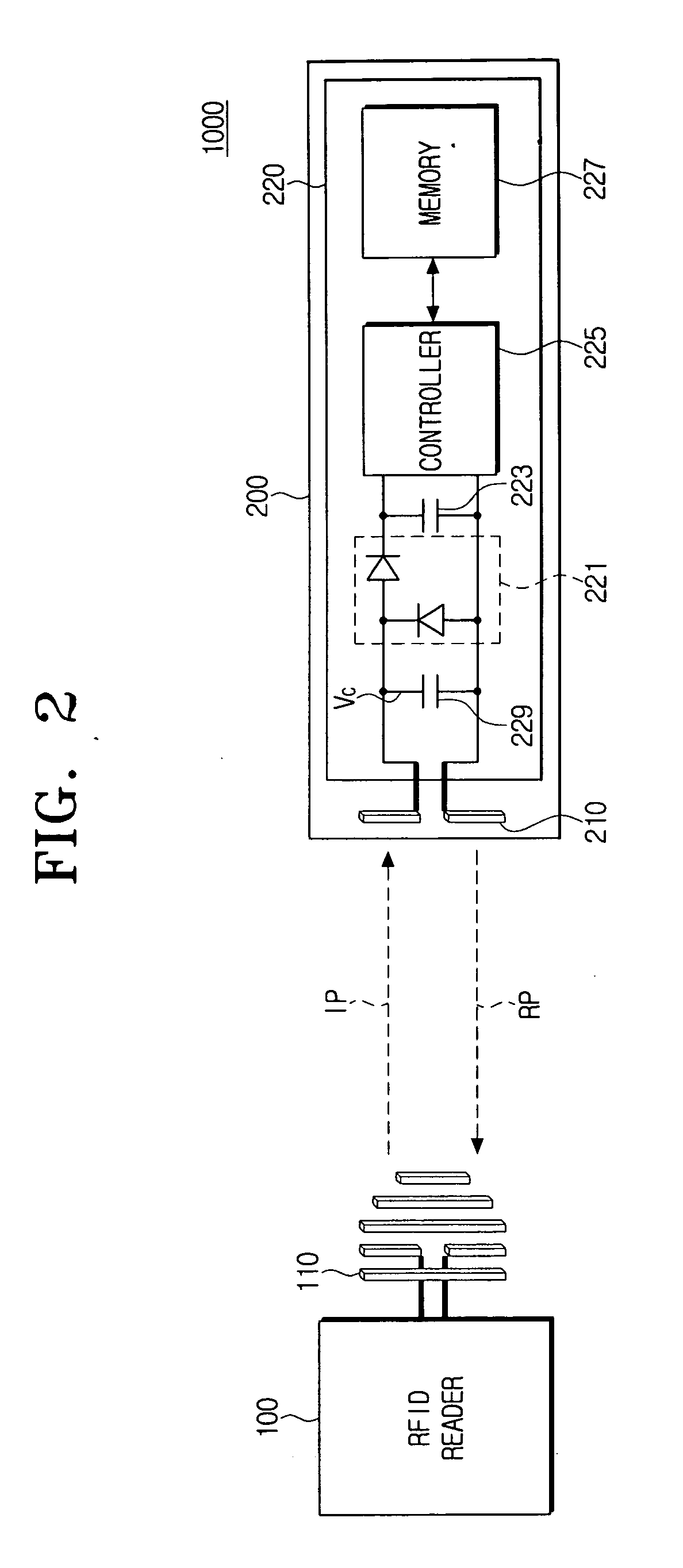
[0044]FIG. 2 is a schematic diagram illustrating an RFID system according to an exemplary embodiment of the present invention.
[0045]Referring to FIG. 2, the RFID system 1000 according to an exemplary embodiment of the present invention includes an RFID reader 100 and an RFID tag 200.
[0046]More specifically, the RFID reader 100 includes an antenna 110 radiating a radio wave and transmits/receives data to/from the RFID tag 200 using radio frequency.
[0047]The RFID tag 200 stores predetermined data including an identifier (ID) given for each RFID tag to identify each RFID tag. If the RFID tag 200 is located in the read range of the RFID reader 100, that is, in the magnetic field or electrical field, the RFID tag 200 receives waves radiated from the RFID reader 100. The wave output from the RFID reader 100 includes an input power IP to drive the RFID tag 200.
[0048]If the RFID tag 200 receives the input power IP from the RFID reader 100, the RFID tag 200 transmits the data including the ID to the RFID reader 100. That is, the RFID tag 200 transmits a reflection power RP including the data to the RFID reader 100, corresponding to the input power IP.
[0049]In detail, the RFID tag 200 includes a tag antenna 210 transmitting/receiving waves to/from the RFID reader 100 and a tag driver 220 generating the reflection power RP using the input power IP.
[0050]The tag antenna 210 receives an input power IP from the RFID reader 100 to transmit to the tag driver 220, and receives a reflection power RP from the tag driver 220 to radiate to the RFID reader 100. The RFID reader 100 authenticates the RFID tag 200 using the data included in the reflection power RP.
[0051]The tag driver 220 is connected to an input pad and ground pad of the tag antenna 210. In this exemplary embodiment, the tag driver 220 can consist of at least one element.
[0052]The tag driver 220 includes a rectifier 221, a smoother 223, a controller 225, a memory 227 and an accumulation mode capacitor 229.
[0053]The rectifier 221 converts the input power IP from alternating current to direct current. The smoother 223 is connected to the rectifier 221 in parallel and outputs the input voltage by converting an alternating current component of the power output from the rectifier 221 into direct current. The input voltage is used to drive internal elements including the controller 225 and the memory 227.
[0054]The controller 225 receives the input voltage from the smoother 223 and generates a reflection power RP using data stored in the memory 227 and the input power IP. The memory 227 stores the ID to identify the RFID tag 200 and other data.
[0055]More specifically, the controller 225 detects the ID from the memory 227 corresponding to the input power IP and generates a signal wave including the detected ID. The signal wave can carry the ID of the RFID tag 200 and other data.
[0056]The controller 225 modulates and outputs the carrier wave according to the signal wave, corresponding to the input power IP. The controller 225 performs modulation by adjusting a voltage in order for the amplitude of the carrier wave to vary corresponding to the amplitude of the signal wave and this kind of modulation method is called amplitude modulation. The controller 225 modifies the amplitude of the carrier wave by adjusting an output voltage Vc of the tag driver 220, that is, the intensity of the voltage of the carrier power RP, and the amplitude of the signal wave varies according to a digital signal corresponding to the signal wave.
[0057]The modulated carrier wave is included in the reflection power RP and transmitted to the RFID reader 100 through the tag antenna 210. The RFID reader 100 demodulates the carrier wave and reads the ID of the RFID tag 200. Accordingly, the RFID reader 100 authenticates the RFID tag 200.
[0058]As described above, the process in which the RFID tag 200 modulates the carrier wave and transmits the carrier wave to the RFID reader 100 is called backscattering.
[0059]The accumulation mode capacitor 229 is connected to the tag antenna 210 in parallel. The accumulation mode capacitor 229 adjusts the capacitance value corresponding to the value of the output voltage Vc so that the impedance of the tag driver 220 is adjusted.
[0060]That is, the impedance of the tag driver 220 adjusted by the capacitance value of the tag driver 220, the intensity of the current of the tag driver 220 and the intensity of the output voltage Vc.
[0061]More particularly, the tag driver 220 adjusts the amplitude of the carrier wave by adjusting the voltage in the process of modulating the carrier wave. Accordingly, the intensity of the output voltage Vc is adjusted by the size of the amplitude of the modulated carrier wave so that the impedance of the tag driver 220 varies according to the size of the amplitude of the carrier wave.
[0062]However, the impedance of the tag driver 220 has to keep a regular value regardless of the size of the amplitude of the carrier wave for impedance matching with the tag antenna 210. Particularly, when the impedance Zc of the tag driver 220 is a complex conjugate of the impedance Za of the tag antenna, impedance is precisely matched. This is as shown in Equation 1.
Zc=Za* [Equation 1]
[0063]The tag driver 220 must maintain the impedance of a regular value for impedance matching with the tag antenna 210, but the impedance Zc of the tag driver 220 can be changed according to the amplitude of the modulated carrier wave.
[0064]To prevent this, the accumulation mode capacitor 229 adjusts its capacitance value corresponding to the output voltage so that the tag driver 220 can maintain the regular impedance regardless of the intensity of the output voltage Vc. That is, in the accumulation mode capacitor 229, if the output voltage Vc increases, the capacitance value decreases, and if the output voltage Vc decreases, the capacitance value increases.
[0065]Accordingly, the capacitance value of the accumulation mode capacitor 229 is inversely proportional to the intensity of the output voltage Vc and the accumulation mode capacitor 229 compensates impedance variation occurred due to the intensity difference of the output voltage Vc. Therefore, the tag driver 220 can maintain the impedance regular regardless of the size of the amplitude of the modulated carrier wave.
[0066]As described above, the RFID tag 200 adjusts the impedance by adjusting the capacitance value according to the size of the amplitude of the carrier wave, so that the intensity of the voltage and current transmitted from the tag driver 220 does not need to be adjusted for impedance adjustment. Accordingly, the RFID tag 200 can prevent the output voltage Vc transmitted from the tag driver 220 from being lower than the reference voltage, and modulation and demodulation can be stably performed so that the reliability of products can be enhanced.
[0067]In addition, as the RFID tag 200 does not need a transistor to adjust the impedance, power consumption by turning on/off the transistor can be prevented and the low-power RFID tag 200 can be implemented.
[0068]Furthermore, since the RFID tag 200 can enhance impedance matching between the tag antenna 210 and the tag driver 220, the reflection coefficient between the RFID reader 100 and the RFID tag 200 can be reduced. Accordingly, the RFID system 1000 can enhance power use efficiency and extend the read range of the RFID reader 100.
[0069]FIG. 3 is a perspective view illustrating a varactor applied to the accumulation mode capacitor of FIG. 2, and FIG. 4 is a circuit diagram illustrating the varactor of FIG. 3.
[0070]Referring to FIGS. 2 to 4, the accumulation mode capacitor 229 includes at least one metal oxide semiconductor (MOS) varactor 229a. The varactor 229a is a variable capacitance diode whose capacitor's value varies according to the input voltage.
[0071]More specifically, the varactor 229a includes a gate part G formed on a base substrate B, a source part S and a drain part D. The area adjacent to where the gate part G is formed on the base substrate B is doped with n+. The output voltage Vc is transmitted to the gate part G. The source part S and the drain part D are electrically connected to each other, and a line which connects the source part S and the drain part D is electrically connected to the gate part G.
[0072]If the output voltage Vc to be input to the gate part G in the varactor 229a is transmitted lower than a threshold voltage, the capacitance value increases. However, if the output voltage Vc to be input to the gate part G in the varactor 229a is transmitted higher than a threshold voltage, the capacitance value decreases.
[0073]FIG. 5 is a graph illustrating the relation between capacitance and source part-gate part voltage in the accumulation mode capacitor of FIG. 2.
[0074]Referring to FIGS. 4 and 5, in the accumulation mode capacitor AV, the higher the voltage Vsg between the source part S (shown in FIG. 4) and the gate part G (shown in FIG. 4) is, the lower the capacitance value is.
[0075]Meanwhile, in the P-MOS capacitor PV, when the voltage between source part S and gate part G ranges from about −1V to about 1V, the capacitance value gradually decreases. However, when the voltage between source part S and gate part G is higher than about 1V, the capacitance value sharply increases.
[0076]Referring to FIG. 2, when the reflection power RP is higher than the reference power, the capacitance value of the accumulation mode capacitor 229 is changed. The reference power is a minimum power by which the RFID reader 100 can read the RFID tag 200 and is also a minimum power Pbs required for backscattering.
[0077]Hereinafter, the process of calculating the minimum power Pbs is described in detail.
[0078]Equation 2 below is an equation to calculate the minimum power Pbs using current values I1 and I2 of the tag driver 220 and a resistance of the tag antenna 210.
P bs = I 1 - I 2 2 8 × R rad [ Equation 2 ]
In Equation 2, I1 and I2 are the current of the tag driver 220, and Rrad is the radiation resistance of the tag antenna 210. Hereinafter, for convenience sake, when the digital signal value corresponding to the signal wave is 0, the current of the tag driver 220 is referred to as the first current I1, and when the digital signal value corresponding to the signal wave is 1, the current of the tag driver 220 is referred to as the second current I2.
[0079]The first and second currents I1 and I2 are calculated using Equation 3 below.
I 1 = V a Z a + Z 1 = V a 2 × R a × ( 1 - ρ 1 ) I 2 = V a Z a + Z 2 = V a 2 × R a × ( 1 - ρ 2 ) [ Equation 3 ]
In Equation 3, Va is the voltage transmitted to the tag antenna 210 by the input power IP, Za is the impedance of the tag antenna 210, and Z1 and Z2 are the impedances of the tag driver 220. Hereinafter, for convenience sake, when the digital signal value of the signal wave is 0, the impedance of the tag driver 220 is referred to as the first impedance Z1, and when the digital signal value of the signal wave is 1, the impedance of the tag driver 220 is referred to as the second impedance Z2.
[0080]Accordingly, I1 and I2 can be calculated using the voltage Va transmitted to the tag antenna 210, the real number impedance Ra of the tag antenna 210, and the first and second reflection coefficients ρ1 and ρ2. When the digital signal value corresponding to the signal wave is 0, the reflection coefficient is referred to as the first reflection coefficient ρ1, and when the digital signal value corresponding to the signal wave is 1, the reflection coefficient is referred to as the second reflection coefficient ρ2. The first and second reflection coefficients ρ1 and ρ2 are calculated through Equation 4 below.
ρ 1 = Z 1 - Z a * Z 1 + Z a ρ 2 = Z 2 - Z a * Z 2 + Z a Z 1 = Z 2 = Z a * [ Equation 4 ]
[0081]The impedances Z1 and Z2 of the tag driver 220 may be complex conjugate values of the impedance Za of the tag antenna 210 for impedance matching with the tag antenna 210. As described above, the impedances Z1 and Z2 of the tag driver 220 have to be equal to complex conjugate values of the impedance Za of the tag antenna 210 regardless of the amplitude of the signal wave for impedance matching with the tag antenna 210. To this end, the accumulation mode capacitor 229 adjusts the capacitance value according to the amplitude of the signal wave to make the first and second impedances Z1 and Z2 equal.
[0082]The average power to drive the tag driver 220 is lower than approximately 50% of an effective power Pa. The effective power Pa is a power provided from the tag antenna 210 to the tag driver 220 and indicates effective isotropic radiated power (EIRP) of the tag antenna 210. Additionally, the minimum power Pbs of the tag driver 220 is lower than approximately 25% of the effective power Pa. Accordingly, the minimum power Pbs is calculated through Equation 5 below.
P bs = P a 4 × ρ 1 - ρ 2 2 = 10 - 10 W = - 70 dBm ( ρ 1 - ρ 2 ) 1 10 5 [ Equation 5 ]
Only when ρ1−ρ2 is over
[0083] 1 10 5 ,
the RFID reader 100 can recognize the RFID tag 200. The effective power Pa is approximately 4 W.
[0084]Accordingly, the minimum power Pbs of the tag driver 220 is approximately 10−10 W, that is, approximately −70 dBm. That is, when the reflection power RP transmitted from the tag driver 220 is over approximately −70 dBm, the RFID reader 100 can recognize the RFID tag 200. Therefore, the accumulation mode capacitor 229 changes the capacitance value in the state that the reflection power RP is over approximately −70 dBm.
[0085]As can be appreciated from the above description, the RFID tag includes the accumulation mode capacitor which adjusts the capacitance value according to the amplitude of the modulated carrier wave. Accordingly, the RFID tag adjusts the capacitance value to adjust the amplitude of the carrier wave without adjusting the voltage and current transmitted from the tag driver. Therefore, as the RFID tag can adjust the impedance by adjusting the capacitance value, it can prevent the voltage transmitted from the tag driver from being lower than the reference voltage, and modulation and demodulation can be stably performed. As a result, the reliability of products can be enhanced.
[0086]In addition, as the RFID tag does not need a transistor to adjust the impedance, power consumption by turning on/off the transistor can be prevented and a low-power RFID tag can be implemented.
[0087]Furthermore, the tag driver can adjust the capacitance value for precise impedance matching with the tag antenna so that reflection signals between the RFID tag and the RFID reader can be reduced. Consequently, the RFID system can enhance power use efficiency and the read range of the RFID reader can be extended.
[0088]While the invention has been shown and described with reference to certain exemplary embodiments thereof, it will be understood by those skilled in the art that various changes in form and details may be made therein without departing from the spirit and scope of the invention as defined by the appended claims.