
Eureka
For R&D, Eureka makes reading and utilizing patents & technical documents easy.
Eureka AIR
Designed for self-driven R&D workflows. Generate viable solutions, solve complex R&D challenges, empower your innovation with AI.

Eureka Materials
Designed for material experts only. Revolutionize your material R&D, from search, analyze, to developing new materials.

TechResearch
Generate reliable direction feasibility study reports for your R&D in just a few steps.

TechSeek
Discover and master advanced knowledge NOW. Basics, ideas, possibilities, all at once.

TechMind
As an expert in R&D Theories, TechMind can generates customized viable solutions instantly.

TechRisk
Analyze your overall solution with one click, know your potential R&D risks in advance.

TechMonitor
Get weekly tech updates, stay abreast of the latest tech innovations and key insights.
Detection device
- Summary
- Abstract
- Description
- Claims
- Application Information
AI Technical Summary
Benefits of technology
Problems solved by technology
Method used
Image

Examples
first embodiment
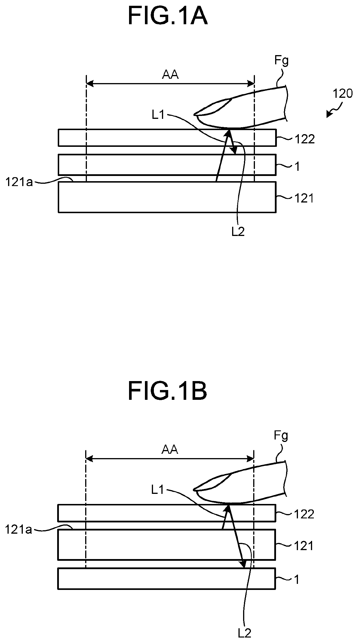
[0090]The following describes a circuit configuration example and an operation example of the detection device 1 according to a first embodiment of the present invention. The description will focus on differences from the comparative example.
[0091]FIG. 7 is a circuit diagram illustrating the detection element according to the first embodiment. As illustrated in FIG. 7, in the configuration of the first embodiment, the photoelectric conversion element 30 is provided between the node N1 and the node N3. The anode of the photoelectric conversion element 30 is coupled to the node N3. The cathode of the photoelectric conversion element 30 is coupled to the node N1. When the light irradiates the photoelectric conversion element 30, the signal (electric charge) output from the photoelectric conversion element 30 is stored in the capacitance Cd of the photoelectric conversion element 30.
[0092]The gate of the first reset transistor Mrst1 is coupled to the reset control scan line GLrst. The o...
second embodiment
[0126]FIG. 10 is a circuit diagram illustrating a detection element according to a second embodiment of the present invention. A detection element 3a according to the second embodiment differs from the detection element 3 described in the first embodiment in that one of the source and the drain of the second reset transistor Mrst2 is coupled to the output signal line SL instead of the coupling point (node N2) between the source of the source follower transistor Msf and the read transistor Mrd. Components having the same functions as those of the first embodiment are denoted by the same reference numerals as those in the first embodiment, and will not be described below. The detection element 3a of the second embodiment will be described mainly in terms of differences from the first embodiment.
[0127]FIG. 11 is a timing waveform diagram illustrating an operation example of the detection element according to the second embodiment. FIG. 12A is a diagram illustrating the equivalent circu...
PUM
 Abstract
Description
Claims
Application Information
 - R&D Engineer
- R&D Manager
- IP Professional
- Industry Leading Data Capabilities
- Powerful AI technology
- Patent DNA Extraction
Browse by: Latest US Patents, China's latest patents, Technical Efficacy Thesaurus, Application Domain, Technology Topic, Popular Technical Reports.
© 2024 PatSnap. All rights reserved.Legal|Privacy policy|Modern Slavery Act Transparency Statement|Sitemap|About US| Contact US: help@patsnap.com