In-situ pad conditioning process for CMP

a polishing pad and in-situ technology, applied in the field of semiconductor device manufacturing, can solve the problems of affecting yield and chip performance, uneven wear, and eroded protrusions on the surface, and achieve the effect of enhancing conditioner performance, discontinuing polishing and removing semiconductor wafers

Inactive Publication Date: 2000-02-08
GOOGLE LLC
View PDF8 Cites 76 Cited by
  • Summary
  • Abstract
  • Description
  • Claims
  • Application Information

AI Technical Summary

Benefits of technology

The present invention provides a method for effectively polishing semi-conductor wafers through use of a specialized polishing pad made from a felt material. This method includes several steps including preparing the polishing pad, positioning the semiconductor wafer on top of it, applying a conditioner with abrasive particles to remove any rough edges or defects, and then rotating the platen to clear away any remaining debris. These technical improvements enhance the quality and efficiency of the polishing process.

Problems solved by technology

The technical problem addressed in this patent is how to improve the efficiency of polishing pads when performing chemical mechanical polishing (CMP) operations. In addition, there is a desire to prevent debris formation on the surfaces of the polishing pad without requiring manual cleaning between each use.

Method used


Image

  • In-situ pad conditioning process for CMP
  • In-situ pad conditioning process for CMP
  • In-situ pad conditioning process for CMP

Examples


Embodiment Construction

)

In describing the preferred embodiment of the present invention, reference will be made herein to FIGS. 1-3 of the drawings in which like numerals refer to like features of the invention. Features of the invention are not necessarily shown to scale in the drawings.

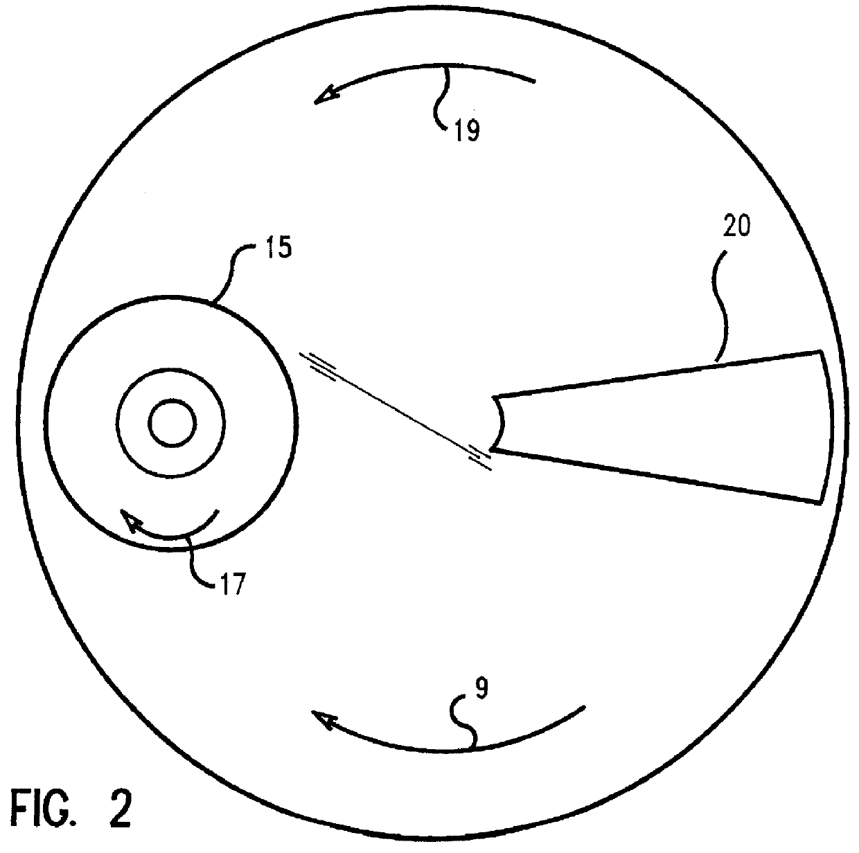
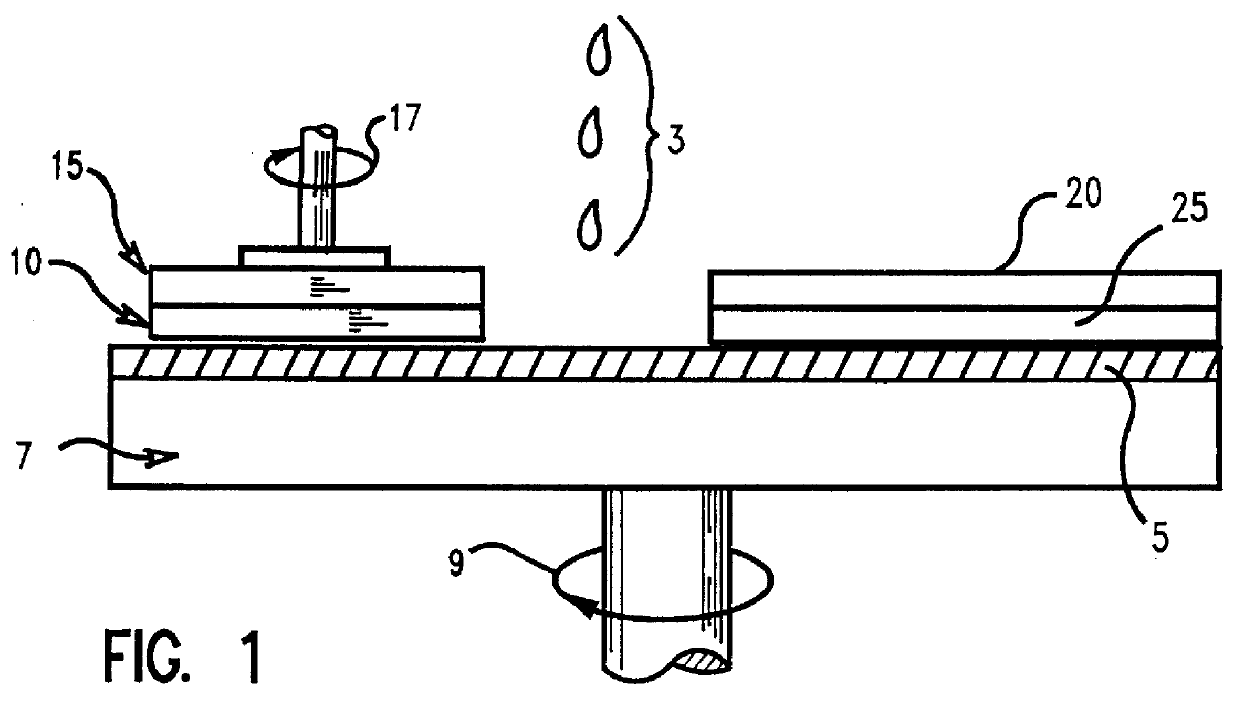
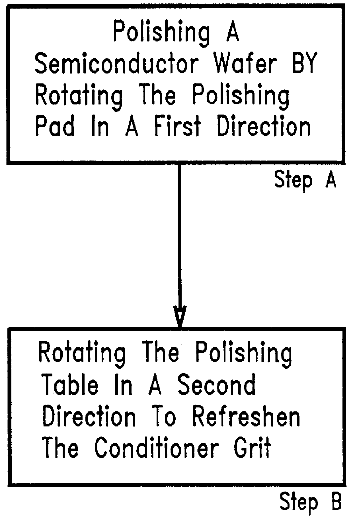
FIG. 1 is an elevational side view of a CMP apparatus which can utilize a method of the present invention. Generally, the CMP apparatus comprises a polishing pad 5 situated on a polishing table or platen 7. Polishing table 7 is linked to a motor which rotates polishing table 7 in a first direction 9 at a rate of about 1 to 100 rpm. An example of a CMP apparatus of this type is the model IC-1000 manufactured by the Rodel Corporation, 945 East San Salvador Drive, Scottsdale, Ariz. 85258.

A wafer holder 15 is employed to hold semiconductor wafer 10 face down against polishing pad 5. The wafer 10 is held in place by applying a vacuum to the back side of wafer 10 or by wet surface tension. A retaining ring (not shown) may be em...


PUM

PropertyMeasurementUnit
Timeaaaaaaaaaa
Timeaaaaaaaaaa

Abstract

An improved method of in-situ conditioning of a polishing pad for use with a stationary pad conditioner during chemical mechanical polishing is described. A polishing table having a polishing pad on its surface is rotated in a first direction during polishing of a semiconductor wafer. A polishing pad conditioner is adjustably attached to the rotating polishing table such that the conditioner is stationary in relation to the rotating polishing table. The conditioner has a roughened surface which is in contact with the polishing pad providing in-situ conditioning during polishing of a semiconductor wafer. After polishing of the semiconductor wafer, the polishing table is rotated in a second direction while the conditioner is still in contact with polishing pad. Rotating the polishing pad in a second direction dislodges the polishing debris clogging the roughened surface of the conditioner and redistributes CMP slurry. The roughened surface of the pad conditioner is refreshed allowing more effective conditioning of the polishing pad. Pad life is prolonged, polishing is stabilized, and the polish cycle time is reduced.

Description


Claims


Application Information

Patent Timeline
Owner GOOGLE LLC
Why Eureka
Try Eureka